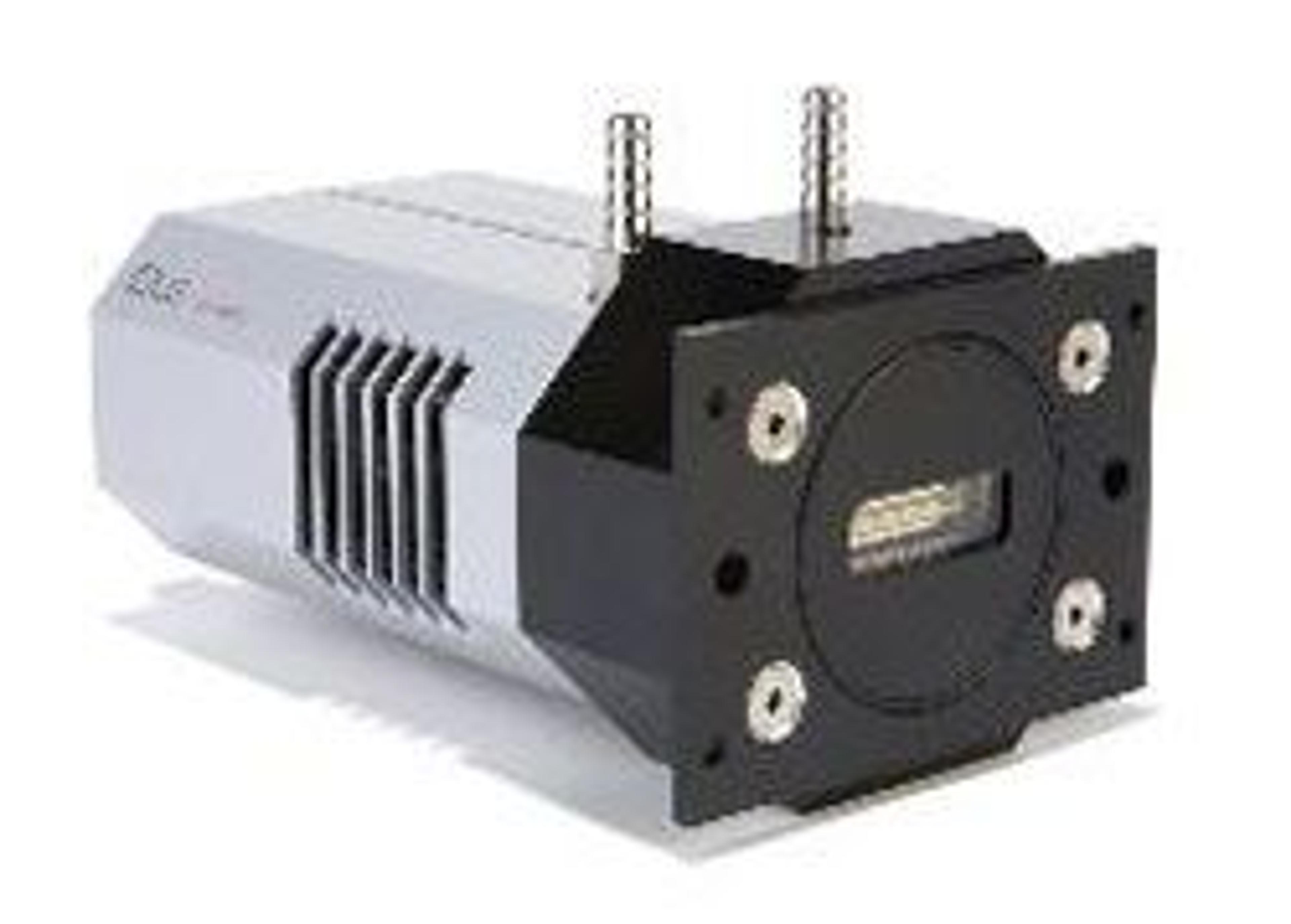
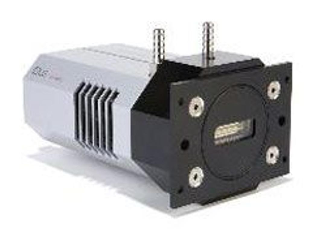
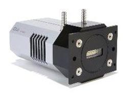
iDus InGaAs CCD Detector
From the manufacturer’s of the World's most compact and reliable spectroscopic CCD detector, comes a new Near Infrared detector solution, the Andor iDus InGaAs detector array system. With all the benefits you’ve come to expect from the iDus range of detectors, the iDus InGaAs detector offers a choice of 512 or 1024 element linear photodiode arrays (PDA) ideal for NIR spectroscopy with high sensitivity output and high resolutio…

The supplier does not provide quotations for this product through SelectScience. You can search for similar products in our Product Directory.
Excellent camera at a very attractive price.
NIR spectroscopy of single nanoparticles
The camera and its standalone software are very easy to use, and sensitivity and noise levels have been better than specified. The price was much lower than the competition, and not having to deal with liquid nitrogen cooling is convenient. For our application, the small increase in dark signal from running at -80 K, rather than -90 K for a liquid N2 cooled camera is less important than read noise. We are able to obtain good S/N spectra in one second exposures for a single ~20 nm particle heated to ~1800 K. The LabView development tools make it easy to integrate the camera into our instrument control program, and that also did not cost an arm and a leg.
Review Date: 2 Mar 2017 | Oxford Instruments Andor
From the manufacturer’s of the World's most compact and reliable spectroscopic CCD detector, comes a new Near Infrared detector solution, the Andor iDus InGaAs detector array system. With all the benefits you’ve come to expect from the iDus range of detectors, the iDus InGaAs detector offers a choice of 512 or 1024 element linear photodiode arrays (PDA) ideal for NIR spectroscopy with high sensitivity output and high resolution covering wavelengths from 800nm up to 2200nm.
Andor's iDus InGaAs 1.7 Array Detector series provides the most optimized platform for Spectroscopy applications up to 1.7 µm. The TE-cooled, in-vacuum sensors reach cooling temperatures of -90°C where best Signal-to-Noise ratio can be achieved. Indeed dark current will improve moderately below -90°C where scene black body radiation will dominate, while Quantum Efficiency of the sensor will be greatly impacted at these lower temperatures and lead to a lower Signal-to-Noise ratio.
Andor's iDus InGaAs 2.2 Array Detector series provides the most optimized platform for Spectroscopy applications up to 2.2 µm. The TE-cooled, in-vacuum sensors reach cooling temperatures of -90°C where best Signal-to-Noise ratio can be achieved. Indeed dark current will improve moderately below -90°C where scene black body radiation will dominate, while Quantum Efficiency of the sensor will be greatly impacted at these lower temperatures and lead to a lower Signal-to-Noise ratio.

Investigating Blood Glucose Monitoring and Sampling Through Spectral Analysis
This application note presents some of the wavelengths of greatest glucose absorption currently being highlighted in spectral analysis, with the end goal of non-invasive monitoring and sampling of blood glucose levels.
Diffuse Reflectance Spectroscopy and Fluorescence Spectroscopy as Techniques for Identification of Lung Cancers
A group working at the Antoni van Leeuwenhoek hospital in the Netherlands are tackling this problem with the use of biophotonic techniques – namely Diffuse Reflectance Spectroscopy (DRS) and Fluorescence Spectroscopy (FS) – to assess how the accuracy of the diagnostic procedure may be improved. This application note outlines their design and testing of prototype instrumentation for the addition of these photonic based modalities to the standard histopathology technique, and demonstrates their benefit to the final diagnosis.
Raman and Photoluminescence Measurements on Laser Lithographically Written Structures in Silicon
Silicon (Si) plays an important role in semiconductor devices. During manufacturing, the structures in Si are traditionally generated using lithography. Confocal Raman and Photoluminescence (PL) imaging are useful tools for quality assurance to investigate stress and stress induced artifacts in Si of semiconductor devices. This application note describes the performance of system laser scribing, confocal Raman imaging and confocal PL imaging on a crystalline Si sample with a single microscope system.