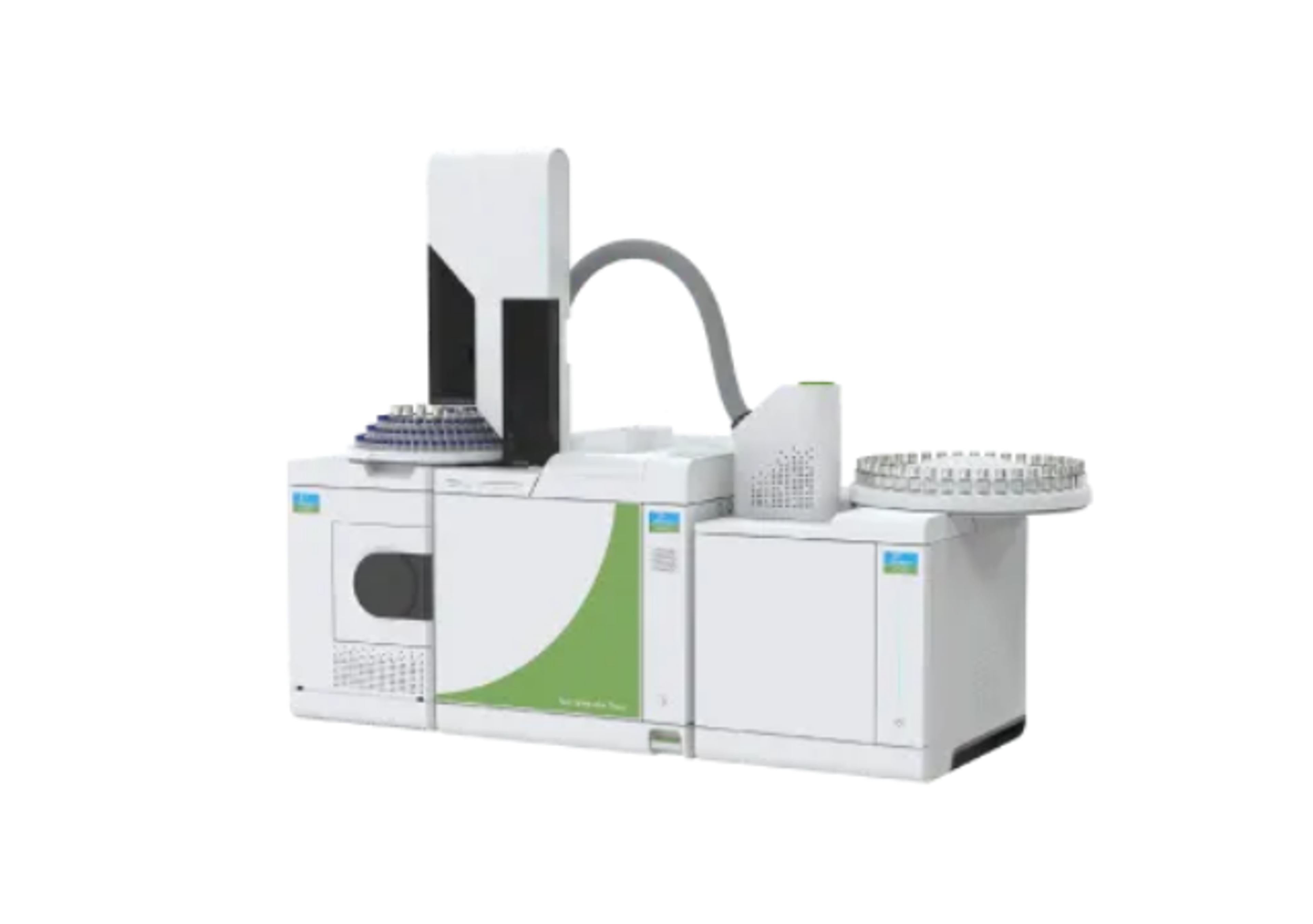
Hysitron PI 89
The Hysitron PI 89 SEM PicoIndenter leverages the advanced imaging capabilities of scanning electron microscopes (SEM, FIBSEM, PFIB), making it possible to perform quantitative nanomechanical testing while simultaneously imaging. Enabled testing techniques include nanoindentation, tensile testing, pillar compression, particle compression, cantilever bending, fracture, fatigue, dynamic testing, and mechanical properties mappin…
Hysitron PI 89 SEM PicoIndenter


The supplier does not provide quotations for this product through SelectScience. You can search for similar products in our Product Directory.
Robust, precise, and modular in-situ SEM nanomechanical testing instrument.
As a leader in nanomechanical testing systems, Bruker makes it easy for you to conduct in-situ mechanical experiments in your scanning electron microscope (SEM) or transmission electron microscope (TEM) with the Hysitron PI Series PicoIndenters. Our unique transducer design delivers unmatched stability throughout your experiments, resulting in precise data even at the nanoscale. Video capture from the microscope enables real-time monitoring and direct correlation of mechanical data to microscope imaging.
Advanced versatility for testing in extreme environments:
- Truly quantitative nanoscale mechanical characterization with direct observation, and up to 3.5 N load and 150 µm displacement
- Encoded XYZ sample positioning with optional tilt and rotation stage
- Modular design supports our full suite of testing techniques, including 1000°C heating, scratch, electrical characterization, scanning probe microscopy (SPM) imaging, XPM property mapping, fatigue/nanodynamic, and more

Time-dependent plasticity in high-temperature pillar compression
Structural materials in demanding applications can be subject both to high stresses and high temperatures simultaneously. The combination of stress and temperature in metals often leads to time-dependent plastic responses, or creep, which can easily lead to premature failure. Creep at temperature is commonly studied with bulk-scale specimens, but can also be done at the microscale. In-situ SEM micro-pillar compression allows specific regions of the microstructure, such as individual grains, to be targeted and allows for high-resolution characterization of the deformation mechanisms.
In this application note, Bruker Nano discusses in-situ SEM micro-pillar compression tests of a Ni-based superalloy, IN718, at 650°C tested with three types of load functions designed to probe the time-dependent response. These include a linear quasistatic loading, a stress relaxation test, and a strain rate jump test. The use of in-situ SEM has additional synergy with high-temperature testing, as the high vacuum of the SEM helps protect the material from oxidation during testing.
Hysitron PI Series PicoIndenters
In this application note, Bruker Nano provides an overview of its Hysitron® PI Series PicoIndenters® for quantitative nanomechanics. These nanomechanical testing systems allow you to conduct in-situ mechanical experiments in your scanning electron microscope (SEM) or transmission electron microscope (TEM). The unique transducer design promises to deliver stability throughout your experiments, resulting in precise data even at the nanoscale. Video capture from the microscope enables real-time monitoring and direct correlation of mechanical data to microscope imaging.
Hysitron PI 89 SEM PicoIndenter
In this application note, Bruker Nano provides a detailed overview of the Hysitron® PI 89 SEM PicoIndenter®. This nanomechanical test instrument leverages the advanced imaging capabilities of scanning electron microscopes (SEM, FIB/SEM), making it possible to perform quantitative nanomechanical testing while simultaneously imaging. Based upon Bruker’s capacitive transducer technology, this new system is the next-generation descendant of the first commercial, in-situ SEM nanomechanics platform.
Direct pull tension testing with the Hysitron PI 89 SEM PicoIndenter - A primer
The tensile test is the most ubiquitous method for macroscale mechanical characterization of materials. This is because it provides a full stress strain curve, allowing analysis of such important material properties as yield strength, ultimate strength, elastic limit, and work hardening rates. In-situ nanomechanical testing is a powerful family of techniques that allow for real-time observation of deformation mechanisms that are directly correlated to load-displacement data.
The combination of these techniques with high-resolution electron microscopy and its related chemical and structural analysis techniques can provide incredibly detailed data. In this application note, Bruker Nano discusses using the Hysitron® PI 89 SEM PicoIndenter® and Tribo iQ™ application for direct pull tension within an SEM application, including the steps required for tip and sample fabrication, tip alignment, and data analysis.
<em>In-situ </em> fiber push-out tests with the Hysitron PI 88 SEM PicoIndenter
In this application note, Bruker Nano utilizes the Hysitron® PI 88 SEM PicoIndenter® equipped with the 800°C heating option to characterize the interfacial strength between individual carbon fibers and the surrounding polyamide matrix, as a function of temperature.
Carbon fiber reinforced polymer composites (CFRPs) possess outstanding mechanical properties including high stiffness, high strength-to-weight ratios, and the ability to withstand dynamic loading in service without catastrophic failure. As a result, CFRPs excel as structural components in numerous applications, especially in the aerospace industry where they are quickly replacing heavier metallic components. The mechanical strength of a composite is a combination of the mechanical properties of the constituent fiber and matrix materials, as well as the strength of the interface between them.
In-situ mechanical testing of semiconductor devices
As advancements are made in the performance of semiconductor devices, changes in materials and processing techniques are often required. The trend towards miniaturizing these devices inherently involves components at or approaching the nanoscale. The mechanical properties of materials at this scale can be vastly different from bulk material, which introduces new concerns both during processing and in field use. A reliable testing technique is critical for evaluating the structural stability of these devices. In this application note, Bruker Nano discusses the use of the Hysitron® PI 85L SEM PicoIndenter® for the investigation of the failure mechanisms involved in FIB-milled back-end-of-line (BEOL) microbeam samples.
In-situ electromechanical testing of ZnO nanowires
In this application note, Bruker Nano presents experimental data on in-situ electromechanical testing of ZnO nanowires. One-dimensional structures such as nanowires and nanotubes are potential materials for future nanoelectronics, optoelectronics, piezoelectric devices, sensors, and actuators. Due to length scale effects and higher surface-to-volume ratios, nanostructures can exhibit superior mechanical and electrical, as well as other length scale-dependent properties. To utilize these fundamental advantages, it is essential to investigate and understand their unique characteristics as a function of the material parameters.
In-situ high-temperature study of a Ni-based superalloy and PtNiAl bond coat
In this application note, Bruker Nano presents an in-situ high-temperature study of a Ni-based superalloy and PtNiAl bond coat. Bond coatings are intermediate layers deposited on superalloy structures to enhance a number of critical performance criteria, including adhesion of a thermal barrier coating, limiting atomic migration of the base metal, and hot corrosion resistance.