In-situ electromechanical testing of ZnO nanowires
6 Jul 2023In this application note, Bruker Nano presents experimental data on in-situ electromechanical testing of ZnO nanowires. One-dimensional structures such as nanowires and nanotubes are potential materials for future nanoelectronics, optoelectronics, piezoelectric devices, sensors, and actuators. Due to length scale effects and higher surface-to-volume ratios, nanostructures can exhibit superior mechanical and electrical, as well as other length scale-dependent properties. To utilize these fundamental advantages, it is essential to investigate and understand their unique characteristics as a function of the material parameters.
Related products
Request Quote for All Products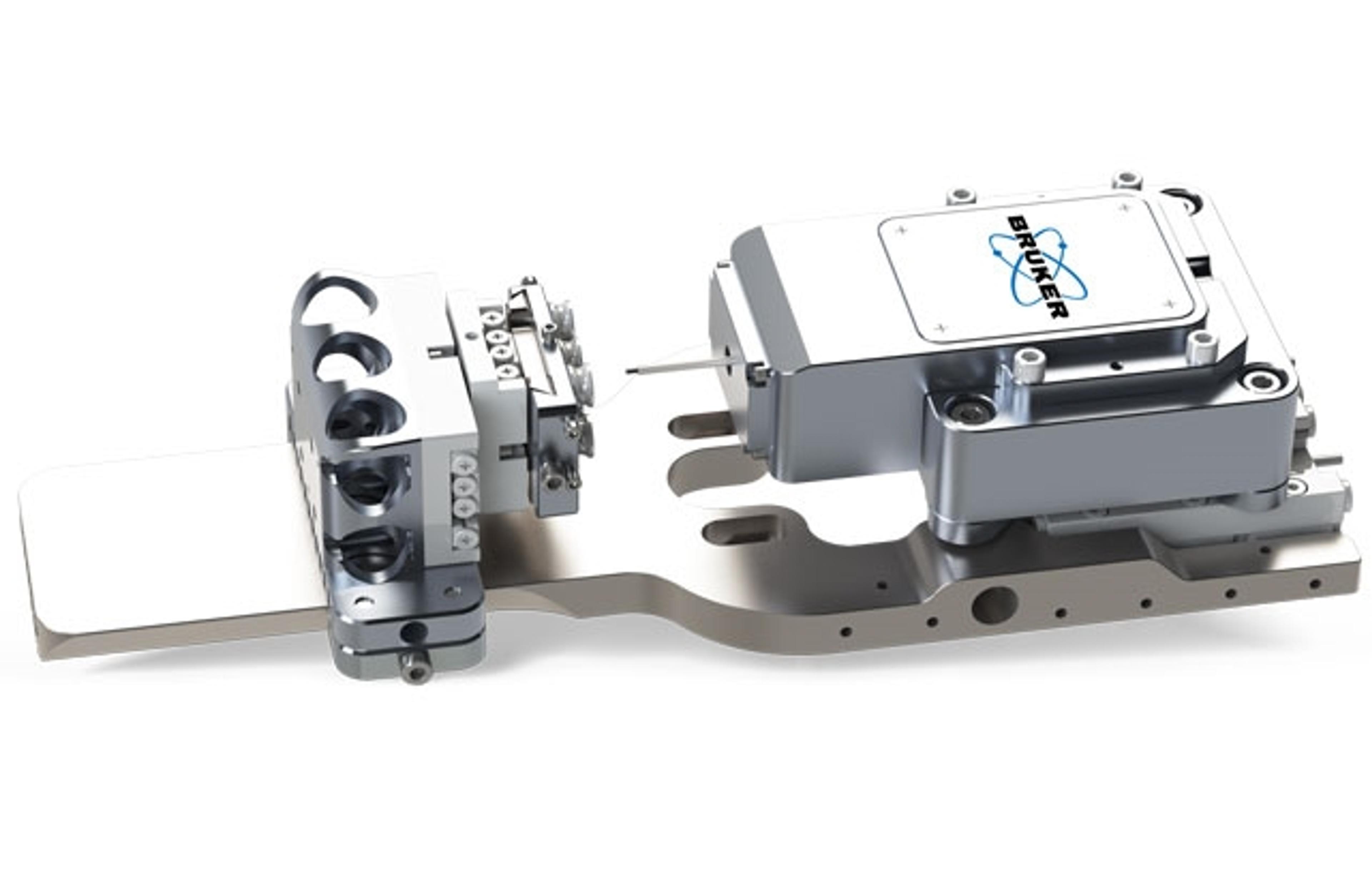
Hysitron PI 89
Bruker Nano Surfaces and MetrologyThe Hysitron PI 89 SEM PicoIndenter leverages the advanced imaging capabilities of scanning electron microscopes (SEM, FIBSEM, PFIB), making it possible to perform quantitative nanomechanical testing while simultaneously imaging. Enabled testing techniques include nanoindentation, tensile testing, pillar compression, particle compression, cantilever bending, fracture, fatigue, dynamic testing, and mechanical properties mapping.