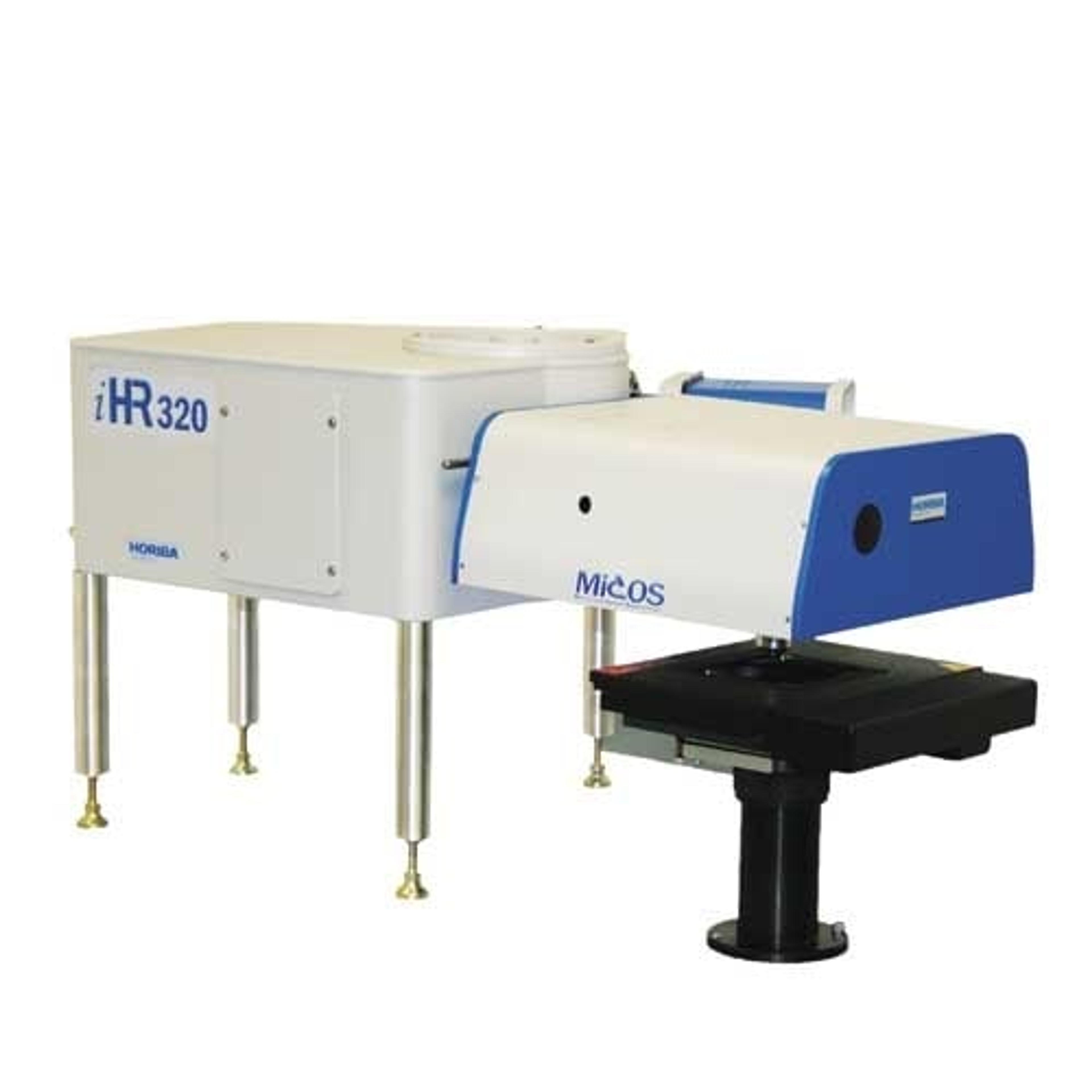
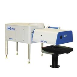
MicOS Microscope Optical Spectrometer
MicOS is a fully integrated and flexible microscope spectrometer that combines a microscope head with a high-performance, triple grating, imaging spectrometer that can accommodate up to 3 different detectors. MicOS is the ideal system for semiconductor microstructure characterization, micro LEDs, micro and macro photoluminescence, photoluminescence mapping of semiconductor wafers.


The supplier does not provide quotations for this product through SelectScience. You can search for similar products in our Product Directory.
We rate it 7/10.
Optical spectrometry
Good quality product. It's after-sale service is satisfactory.
Review Date: 20 Jan 2020 | HORIBA Scientific
MicOS is a fully integrated and flexible microscope spectrometer that combines a microscope head with a high-performance, triple grating, imaging spectrometer that can accommodate up to 3 different detectors. MicOS is the ideal system for semiconductor microstructure characterization, micro LEDs, micro and macro photoluminescence, photoluminescence mapping of semiconductor wafers.

Photoluminescence Characterization of GaN Alloys and Other Semiconductor Microstructures
GaN and related alloys are important materials used to build short-wavelength light sources (lasers and LEDs). Room- and low-temperature photoluminescence (PL) are used to characterize these materials as well as device performance. Parameters such as IQE of quantum wells (QW) can be measured for patterned structures using selective optical excitation of microstructures made from these materials. Selective excitation means fine control of laser-excitation beam size and positioning, and visualization of the sample under measurement.
Room-temperature Micro-electroluminescent Characterization of Ge-based IR Sources
Monolithic integration of optical components on CMOS platforms is ongoing in the optical communications industry. CMOS offers a mature and robust platform, and therefore is logical for building optical-interconnect modules. These modules include light sources, modulators, multiplexers, and detectors on a single substrate. Silicon is the foundational material for CMOS technology, but as a material with an indirect bandgap, it poses a serious obstacle to building light sources via CMOS-based integrated photonics.
III-V Wafer Characterization through Photoluminescence Mapping
III-V semiconductors are important to the fabrication of active photonic devices such as light sources and detectors. Successful fabrication of such devices relies on the high quality of the underlying materials and precise deposition of intended geometries on a wafer substrate. Defective materials and imperfections in geometries adversely affect yield, and usually increase cost and development times. The cost and delay penalties are further compounded when such defects in either material or device-geometry are not caught early enough in the cycle.