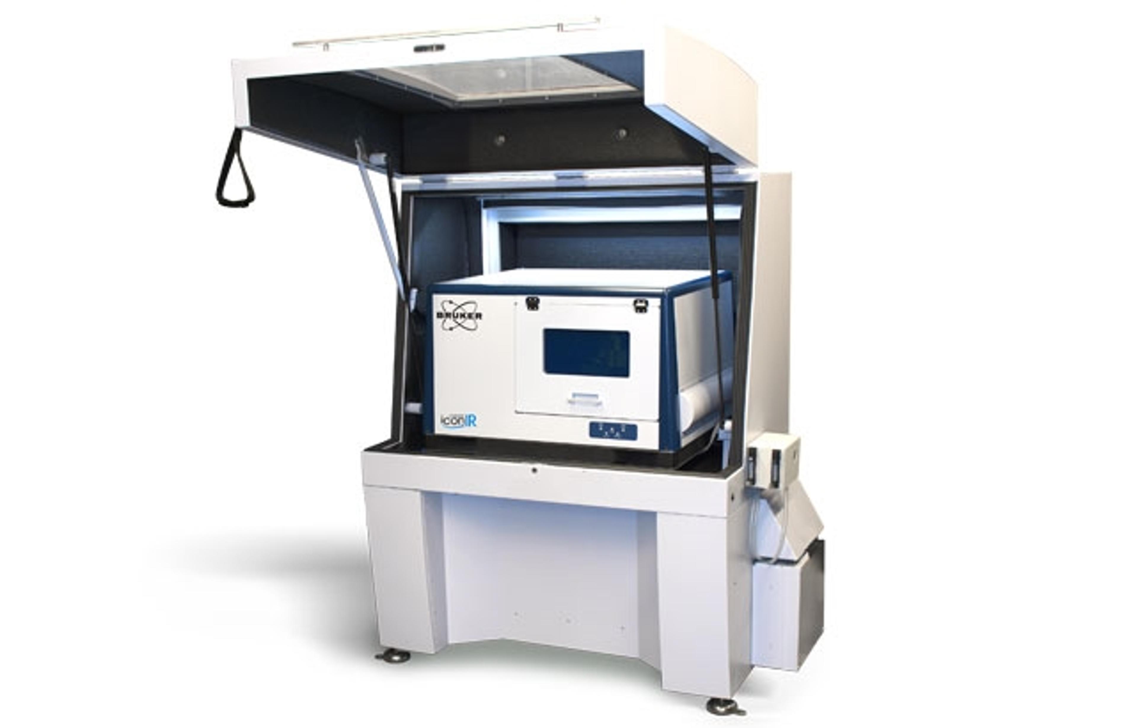
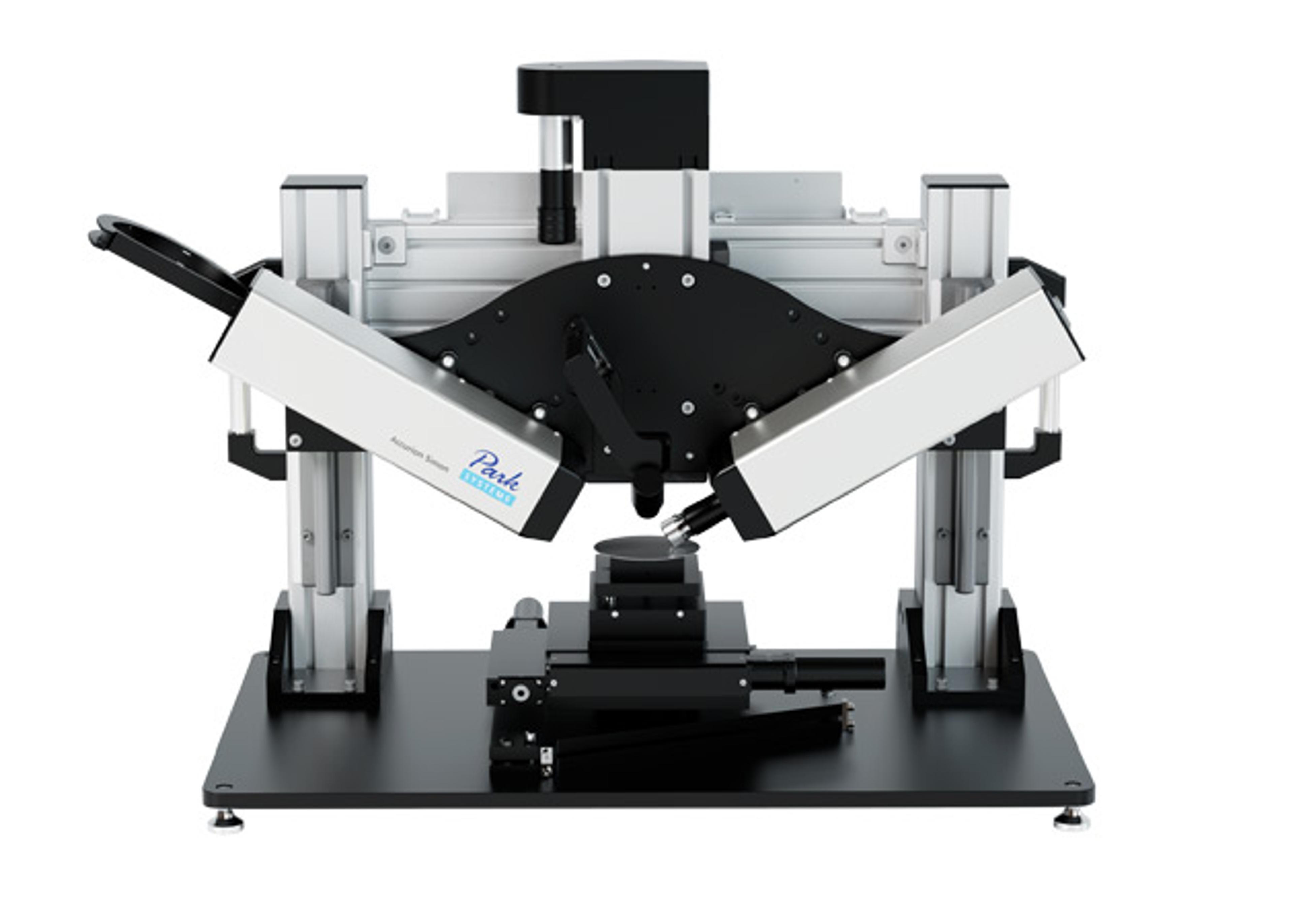
Dimension IconIR
Bruker’s large-sample Dimension IconIR system combines nanoscale infrared (IR) spectroscopy and scanning probe microscopy (SPM) on one platform to deliver the most advanced spectroscopy, imaging, and property mapping capabilities available for academic researchers and industrial users. Incorporating decades of research and technological innovation, IconIR provides unrivaled performance based on and building off the industry-b…

Dimension IconIR AFM-IR spectrometer
The supplier does not provide quotations for this product through SelectScience. You can search for similar products in our Product Directory.
Highest performance, large-sample nanoIR with PeakForce property mapping.
Dimension IconIR utilizes Bruker-exclusive PeakForce Tapping® nanoscale property mapping and proprietary nanoIR spectroscopy technology to enable correlative microscopy for nanochemical, nanoelectrical, and nanomechanical characterization of materials and active nanoscale systems in electrical or chemically reactive environments.
Only Dimension IconIR delivers:
- High-performance nanoIR spectroscopy with FT-IR correlation, <10 nm chemical resolution, and monolayer sensitivity.
- Correlative chemical imaging with PeakForce Tapping nanomechanical and nanoelectrical modes.
- Highest-performance AFM imaging and ultimate sample flexibility.
- The broadest range of applications accessories and AFM modes.
Brochures

Enabling first-and-only nanoIR capabilities and performance with the Dimension IconIR
In this brochure from Bruker, explore the large-sample Dimension IconIR, a combined nanoscale infrared (IR) spectroscopy and scanning probe microscope (SPM) system that delivers spectroscopy, imaging, and property mapping performance on a single platform. Featuring high-resolution chemical imaging with monolayer sensitivity, the system’s large-sample architecture also provides sample flexibility while retaining the AFM measurement capabilities of the Dimension Icon®.
Nanoscale IR spectroscopy of organic contaminants
Organic nano-contaminants are a serious defectivity issue for semiconductor and data storage companies where current characterization techniques have limited capabilities. In this application note from Bruker, learn more about the application of the nanoIR2-FS™ to the measurement of such defects. The nanoIR2-FS system is based on a scientific breakthrough technique of acquiring IR spectra at spatial resolutions down to sub 10 nm, enabling researchers to obtain nanoscale chemical fingerprints of their material. The spectra generated using Bruker nano’s patented AFM-IR™ technique correlate extremely well with traditional FT-IR spectra, and are thus comparable to standard IR libraries. In addition to chemical analysis, the nanoIR2-FS provides complementary mechanical, thermal, and structural property information with nanoscale spatial resolution.
Characterization of advanced semiconductor materials and processes with nanoscale IR spectroscopy
Submicron and nanoscale chemical identification of semiconductor materials, specifically those that are organic, is a significant challenge in the research of devices, as well as in process control and failure analysis environments. In this application note from Bruker, explore how because of these challenges there are a multitude of techniques used by semiconductor manufacturers to identify chemical components.
2D materials characterization using nanoscale FTIR spectroscopy and near-field imaging
2D materials are an important emerging field of research due to their unique properties for applications in photovoltaics, semiconductors, battery technology and many other areas. 2D materials have been characterized by multiple nanoscale and microscopy techniques to gain a better understanding of the nature of their properties. In this application note from Bruker, explore how Nanoscale FTIR techniques extend this characterization with critical chemical and optical data at the nanoscale.
Correlation between nanoscale and bulk thermal analysis
Thermal methods, such as differential scanning calorimetry (DSC) and modulated temperature DSC (MDSC), thermogravimetric analysis (TGA), thermomechanical analysis (TMA), and dynamic mechanical analysis (DMA), are well-established techniques for characterizing the morphology and composition of polymers. It is often possible to identify and quantify materials by their characteristic transition temperatures and thermal stability. However, a serious limitation of conventional thermal methods is that they give only a sample-averaged response and cannot provide information on specific features on or within the sample. A DSC measurement, for example, may indicate the presence of more than one phase, but the technique cannot generally give any information regarding the size or distribution of phases. In this application note from Bruker, explore how this particularly impacts scientists in the field of polymer blends (where the blend morphologies are crucial to determining their material properties), coatings (where imperfections such as gel formations can seriously impact performance), and composites.
High-resolution chemical imaging with tapping AFM-IR
The spatial resolution of conventional bulk infrared (IR) spectroscopy is limited by diffraction to around 3-10 µm, depending on the method used. Atomic force microscopy (AFM) is a widely used nanoscale imaging technique that provides the user with a high spatial resolution topographic map of a sample surface. Until now, the major drawback of AFM has been its inability to chemically characterize the material underneath the tip. AFM-IR is a photothermal technique that combines AFM and IR spectroscopy to unambiguously identify the chemical composition of a sample with tens-of-nanometers spatial resolution. So far, it has been successfully used in contact mode in a variety of applications. However, contact mode has proven unsuitable for soft or loosely adhesive samples, such as the less than 200 nm polymeric nanoparticles (NPs) that are of wide interest for biomedical applications. In this application note from Bruker, explore how AFM-IR overcomes such limitations, bringing the power of both IR spectroscopy and AFM topography mapping to a much wider range of applications.
Chemical characterization of polymeric films, blends, and self-assembled monomers
The spatial resolution of conventional bulk infrared (IR) spectroscopy is limited by Abbe diffraction laws to between 3–10 µm, depending on the method used. Atomic force microscopy (AFM) is a widely used nanoscale imaging technique that provides the user with a high spatial resolution topographic map of a sample surface. Until now, the major drawback of AFM has been its inability to chemically characterize the material underneath the tip. When combined with an IR source, the resulting AFM-IR technique breaks the diffraction limit of conventional IR spectroscopy by orders of magnitude, while still providing the high-resolution imaging capabilities of AFM.1 In this application note from Bruker, explore how AFM-IR is used to address nanoscale chemical characterization on a range of polymeric and thin film samples.
Utilizing nanoscale IR spectroscopy to characterize biological samples in nanoscale detail
The combination of atomic force microscopy (AFM) with infrared spectroscopy (IR) techniques, known as AFM-IR, allows for the chemical characterization of samples in nanoscale detail that would not be possible with the two techniques alone. AFM-IR spectroscopy, or nanoscale IR spectroscopy, has many applications including polymer characterization, pharmaceutical science, microelectronics, and life sciences. In this application note from Bruker, explore the principles and advancements of AFM-IR and see examples of AFM-IR applications in the life sciences, specifically for the nanoscale characterization of biological samples including proteins, structures within single cells, monolayers, and tissues.
Spatiospectral nanoimaging of surface phonon plasmons
With their high spatial confinement, surface plasmon polaritons (SPPs) and surface phonon polaritons (SPhPs) in 2D materials can open up new opportunities to enhance light-matter interaction and enable the development of super lenses, subwavelength metamaterials, and other novel photonic devices. In-situ characterization of these polaritonic excitations across different applications requires a versatile optical imaging and spectroscopy tool with nanometer spatial resolution and wide spectral coverage. In this application note from Bruker, explore how through a noninvasive near-field light-matter interaction, scattering-type scanning near-field optical microscopy (s-SNOM) provides a unique way to selectively excite and locally detect electronic and vibrational resonances in real space.