2D materials characterization using nanoscale FTIR spectroscopy and near-field imaging
27 Jun 20232D materials are an important emerging field of research due to their unique properties for applications in photovoltaics, semiconductors, battery technology and many other areas. 2D materials have been characterized by multiple nanoscale and microscopy techniques to gain a better understanding of the nature of their properties. In this application note from Bruker, explore how Nanoscale FTIR techniques extend this characterization with critical chemical and optical data at the nanoscale.
Related products
Request Quote for All Products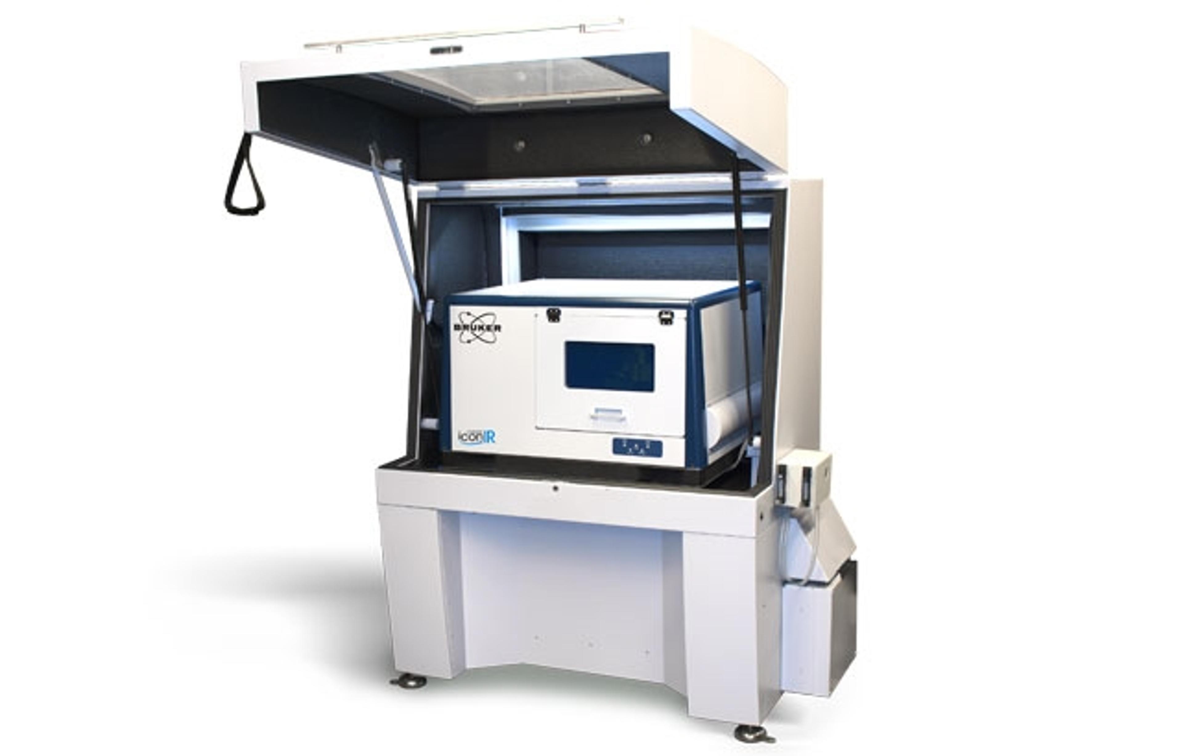
Dimension IconIR
Bruker Nano Surfaces and MetrologyBruker’s large-sample Dimension IconIR system combines nanoscale infrared (IR) spectroscopy and scanning probe microscopy (SPM) on one platform to deliver the most advanced spectroscopy, imaging, and property mapping capabilities available for academic researchers and industrial users. Incorporating decades of research and technological innovation, IconIR provides unrivaled performance based on and building off the industry-best AFM measurement capabilities of the Dimension Icon.
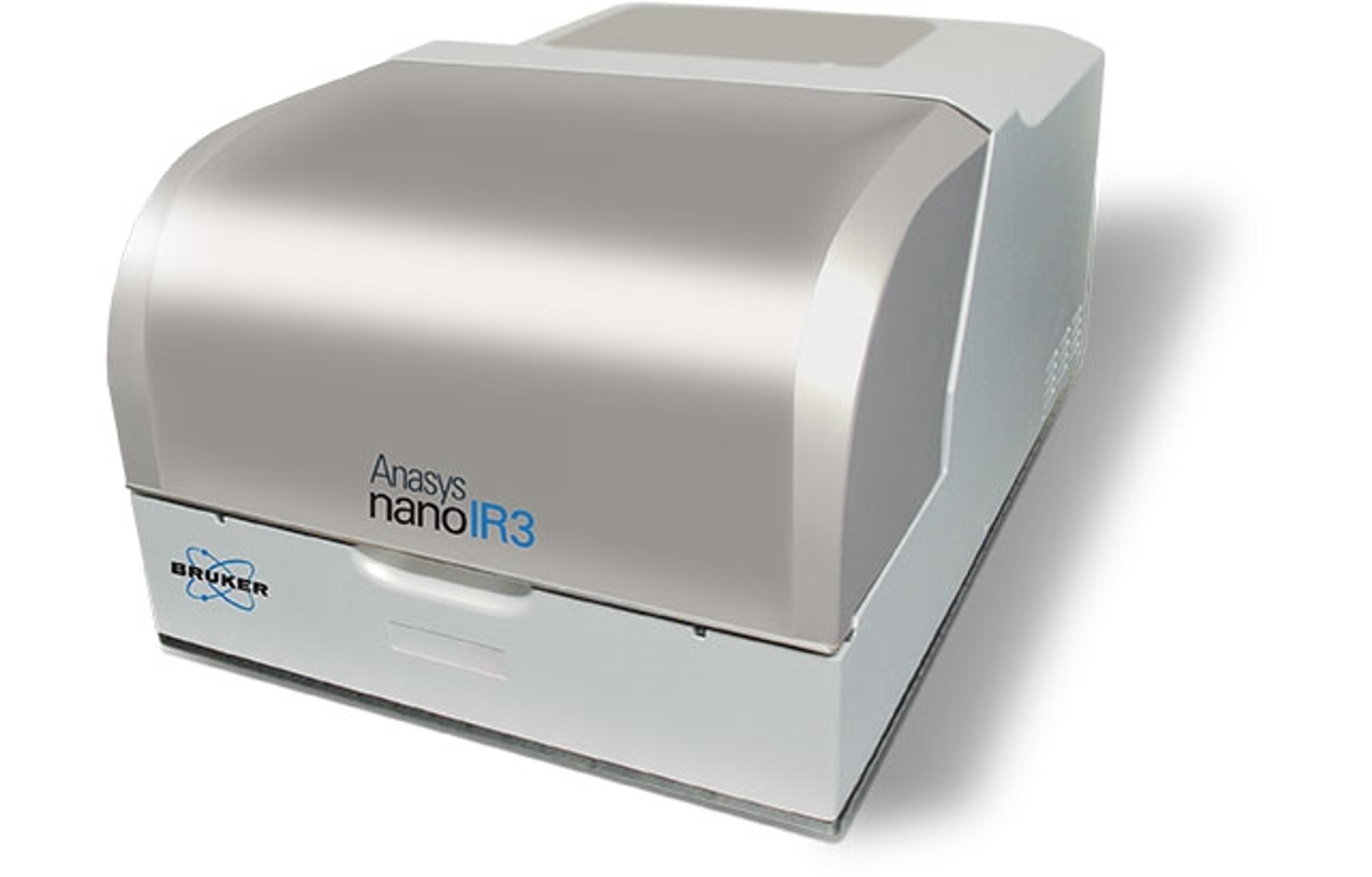
Anasys nanoIR3
Bruker Nano Surfaces and MetrologyThe nanoIR3 is the latest generation nanoscale IR spectroscopy, chemical imaging, and property mapping system for both materials and life science applications. The system also provides IR-based chemical imaging to provide mapping of chemical variations of the feature of interest. Unique point spectroscopy capabilities provide both spectroscopy and chemical imaging with a single source.