NewsMaterials
MATERIALS UPDATE: Mounting Possibilities for Graphene and 2D Materials
29 Jul 2018
Lui Terry
Administrator / Office Personnel
Editorial article
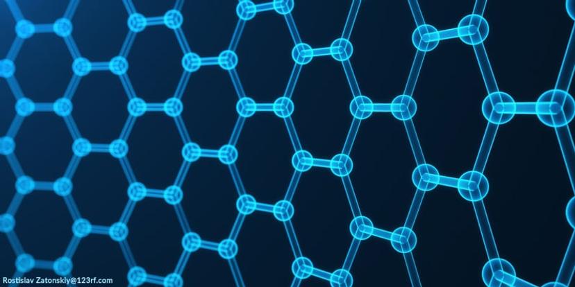
Graphene and other 2D materials are undoubtedly hot topics in the scientific community. With an increasing number of developments in areas of analysis, characterization and research over recent months, the likelihood of delivering on the promise shown by these materials is growing. From the development of a dedicated graphene characterization service for industry to integrated analysis techniques, SelectScience® brings together all the latest news, application notes and videos relevant to the graphene and 2D materials community.
Related products
Request Quote for All Products
Links
Tags
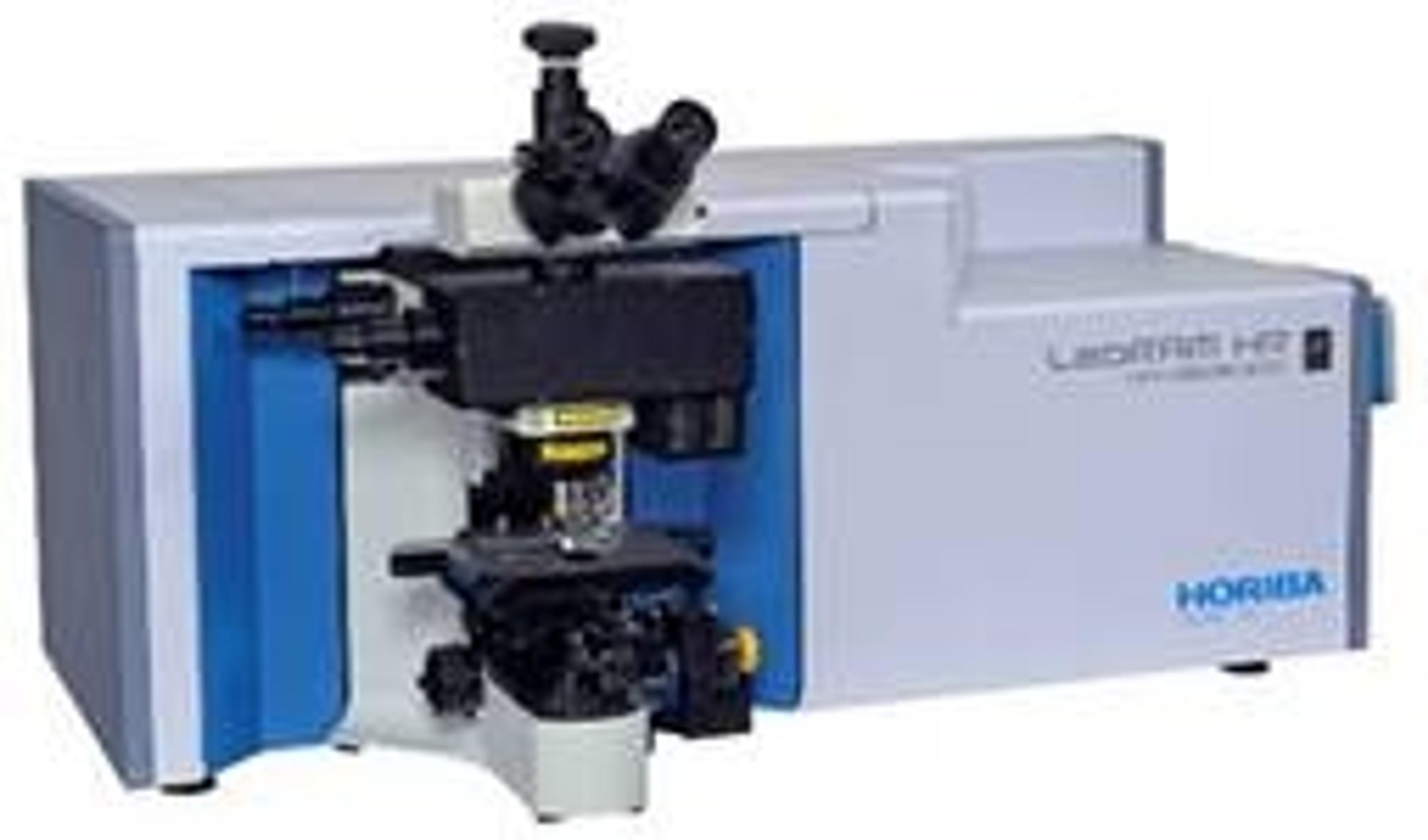
Fluorescence SpectroscopyFluorometers and spectrofluorometers (also called fluorescence spectrometers) are used to measure the intensity and wavelength of fluorescent light emitted from a sample after excitation by illumination. Spectrofluorometers utilize monochromators to select the desired wavelengths, whereas filter fluorometers employ a set of filters. Spectrofluorometers for measuring steady-state fluorescence and lifetime fluorescence (or time-resolved fluorescence) are available, as well as fluorescence microscopes and microplate readers. Find the best fluorescence spectroscopy products in our peer-reviewed product directory: compare products, check customer reviews and receive pricing direct from manufacturers.Raman SpectroscopyRaman spectroscopy is used to discern the vibrational and rotational states of molecules and hence the chemical composition of a sample by measuring the inelastic scattering of monochromatic light. Explore a range of Raman spectrometers, including handheld/portable Raman spectrometers for QC/QA labs and in situ spectrometers for processes. Conduct Raman imaging for microanalysis of mixed samples using a Raman microscope. Raman spectrographs are also available. Find the best Raman spectroscopy products in our peer-reviewed product directory: compare products, check customer reviews and receive pricing direct from manufacturers.UV-Visible SpectroscopyUltraviolet-visible (UV-Vis) spectrophotometers are used to measure the interaction of UV and visible light with a sample, including transmission, reflectance & absorbance. The two major instrument classes are single-beam or double-beam spectrophotometers. More specialized equipment includes colorimeters, spectroradiometers and refractometers. Portable and microvolume spectrophotometers are also available. For the modular spectroscopy lab, explore a range of light sources for combination with a spectrograph/spectrometer and optics. Find the best UV-Vis spectroscopy products in our peer-reviewed product directory: compare products, check customer reviews and receive pricing direct from manufacturers.NanotechnologyNanotechnology, or nanotech, is an engineering technique using molecular scale functional systems. Applications of nanotechnology include medicine and medical devices, electronics, air and water purification, food science and energy production.ProfilometersProfilometers are instruments used to measure a surface's profile, in order to quantify etch depth, deposited film thickness, and surface roughness. They operate in either contact or non-contact modes and may use optical or stylus techniques to make the actual measurements.Electron MicroscopyElectron microscopes (EM) are used to create high-resolution images of samples at the nanoscale by means of an accelerated beam of electrons as a source of illumination. Types of electron microscope include scanning electron microscopes (SEM), transmission electron microscopes (TEM), scanning transmission electron microscopes (STEM) and cryo-electron microscopes. Focused ion beam (FIB) microscopes are useful for modifying or milling a sample surface with nanometer precision, as well as imaging. Find the best electron microscopes in our peer-reviewed product directory: compare products, check customer reviews and receive pricing direct from manufacturers.Atomic Force Microscopy / Scanning Tunneling MicroscopyAtomic force microscopes (AFM) and scanning tunneling microscopes (STM) are high-resolution forms of scanning probe microscope (SPM) used to generate topological information of a sample down to the atomic scale. Instruments can generate an image of the surface topology, manipulate objects and reveal information on localized properties such as Young’s modulus, conductivity, and magnetism. High-quality STM and AFM probes optimized for your application are available, as well as other SPM-based instruments such as scanning ion conductance microscopes (SICM) & near-field scanning optical microscopes (NSOM). Find the best AFM and STM equipment in our peer-reviewed product directory: compare products, check customer reviews and receive pricing direct from manufacturers.GrapheneGraphene is a two-dimensional structure that comprises of a hexagonal honeycomb lattice of carbon atoms. Graphene can conduct electricity and heat, is almost transparent and is 100x stronger than steel by weight.2D Materials