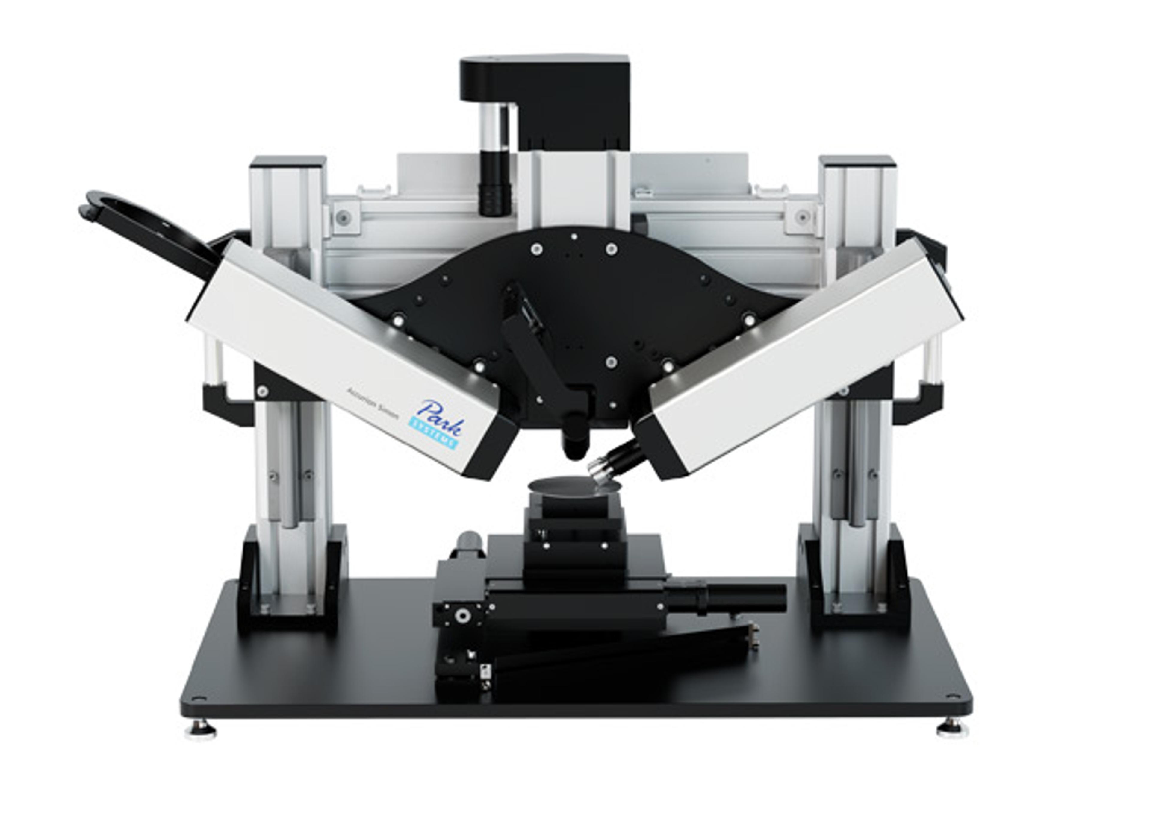
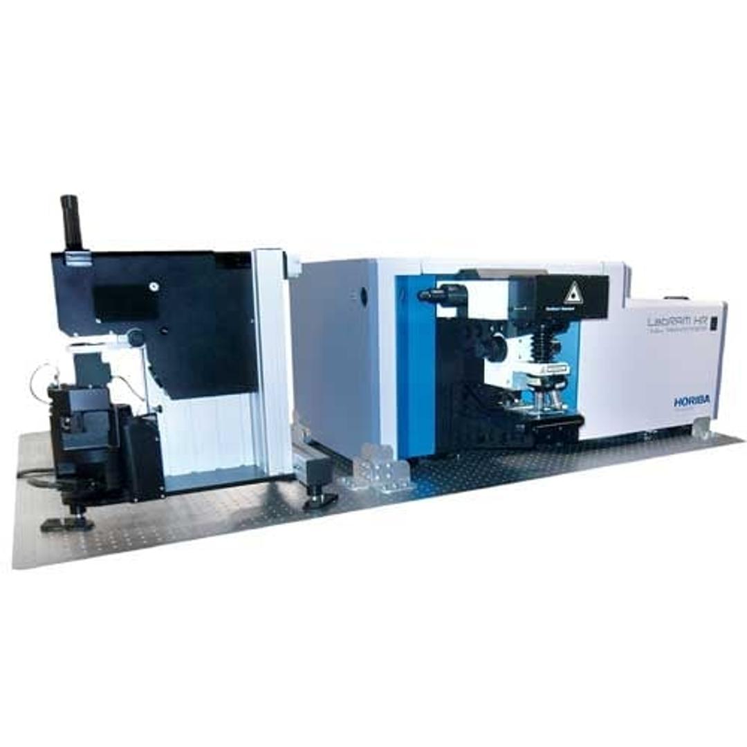
HR Evo Nano
The Ultimate Nano-Spectroscopy Solutions

The supplier does not provide quotations for this product through SelectScience. You can search for similar products in our Product Directory.
The HR Evo Nano brings ease-of-use and extreme flexibility together for the most demanding AFM/Raman applications, including nanotechnology, materials science, 2D materials, and more.
With capabilities from deep UV to infrared, high spectral resolution, and an extended set of options and accessories, the HR Evo Nano is ideally suited to perform in any of your research challenge.

Characterization of MoS<sub>2</sub> Flakes using Tip-Enhanced Optical Spectroscopies (TEOS)
Molybdenum disulfide (MoS2) is a promising semiconducting Transition Metal Dichalcogenide (TMD) 2D nano-material for next generation photovoltaic solar cells, optoelectronic circuits and sensors due to its great excitonic recombination property, high carrier mobility and low leakage current. One of the advantages of two dimensional (2D) TMDs, when compared to graphene, comes from quantum confinement, enabling the indirect-to-direct bandgap transition as a function of number of individual layers. Nano-scale characterization is needed for the understanding necessary to engineer nanodevices integrating monolayer MoS2.
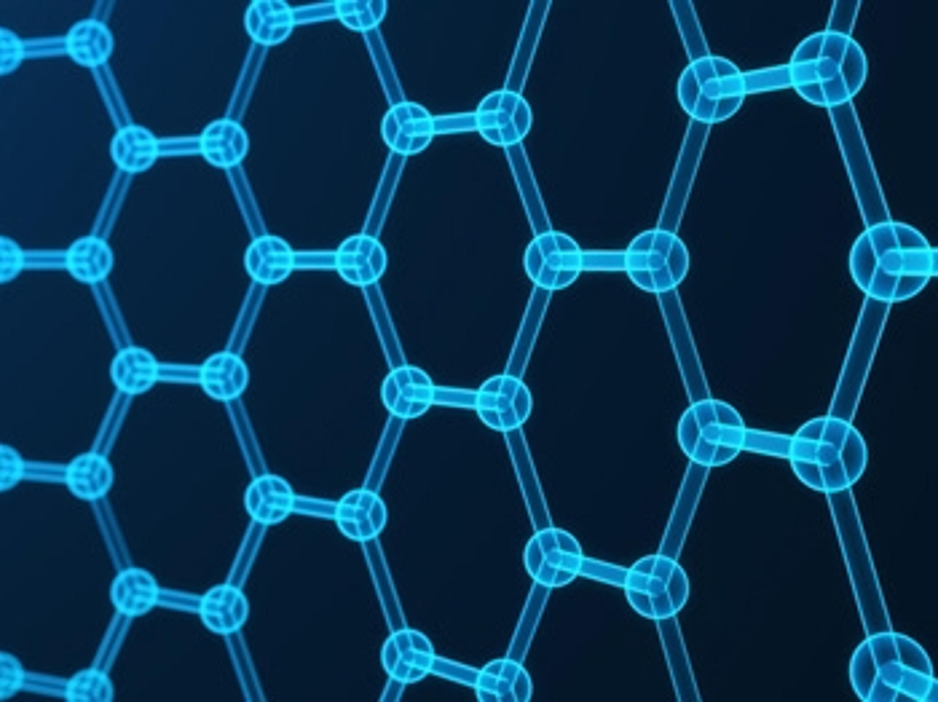
Characterization of Graphene using Tip-Enhanced Raman Spectroscopy (TERS)
Graphene is a crystalline bi-dimensional material made of an atomically thick layer of sp2-bonded carbon atoms arranged in a honeycomb lattice. It was discovered in 2004 by A. Geim and K. Novoselov who received the Nobel Prize in 2010. Graphene has extraordinary properties, in particular, extremely high electron mobility, which opens up a large variety of applications in nanoelectronics, optoelectronics, and batteries. Strangely, the high electric conductivity of graphene has hindered its integration, but the recent development of semiconductor 2D materials, and their potential combination with graphene, has revived the integration of graphene into nanoelectronics devices. While graphene oxide was primarily considered as an intermediate form for large scale production of graphene due to its easy dispersability in water, graphene oxide is also of interest for a lot of applications as it can be functionalized or used as a non-conductive layer.
Characterization of Carbon Nanotubes using Tip-Enhanced Raman Spectroscopy (TERS)
Carbon nanotubes are now manufactured in large volumes (several thousand tons per year) and are present in many daily life products ranging from car parts, batteries, and sports equipment, to water filtration systems and boat equipment. Nevertheless, there is still a long way to go to produce single wall carbon nanotubes in large scale devices with exceptional theoretical electrical and thermal conductivities and mechanical resistance. Additional knowledge is essential for boosting CNT integration into thin film microelectronics, optoelectronics, and medical devices.
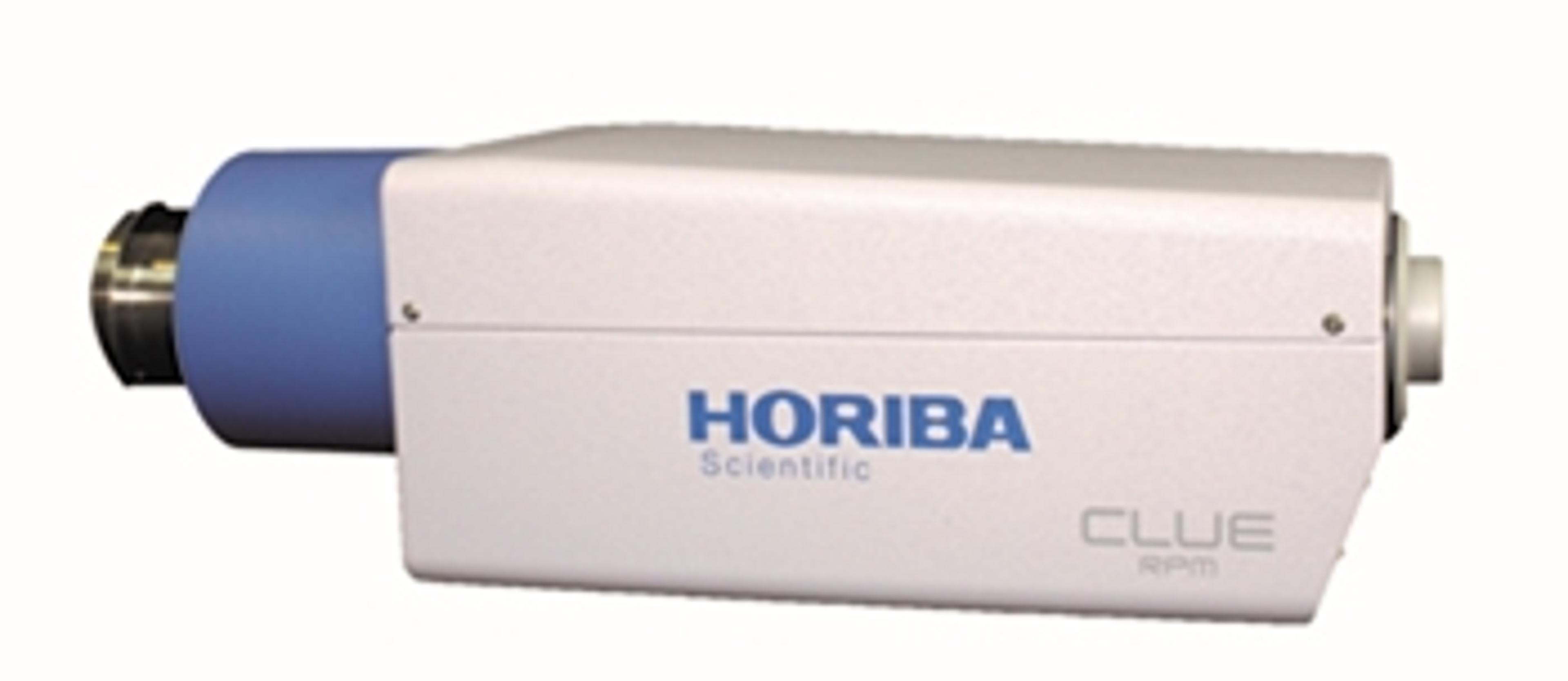
HORIBA Scientific Introduces New CLUE Series Detectors for Scanning Electron Microscopes
CLUE Series offers scalable platform for imaging and spectroscopic analysis of nano-objects with SEM and dual SEM/FIB (Focused Ion Beam) microscopes.