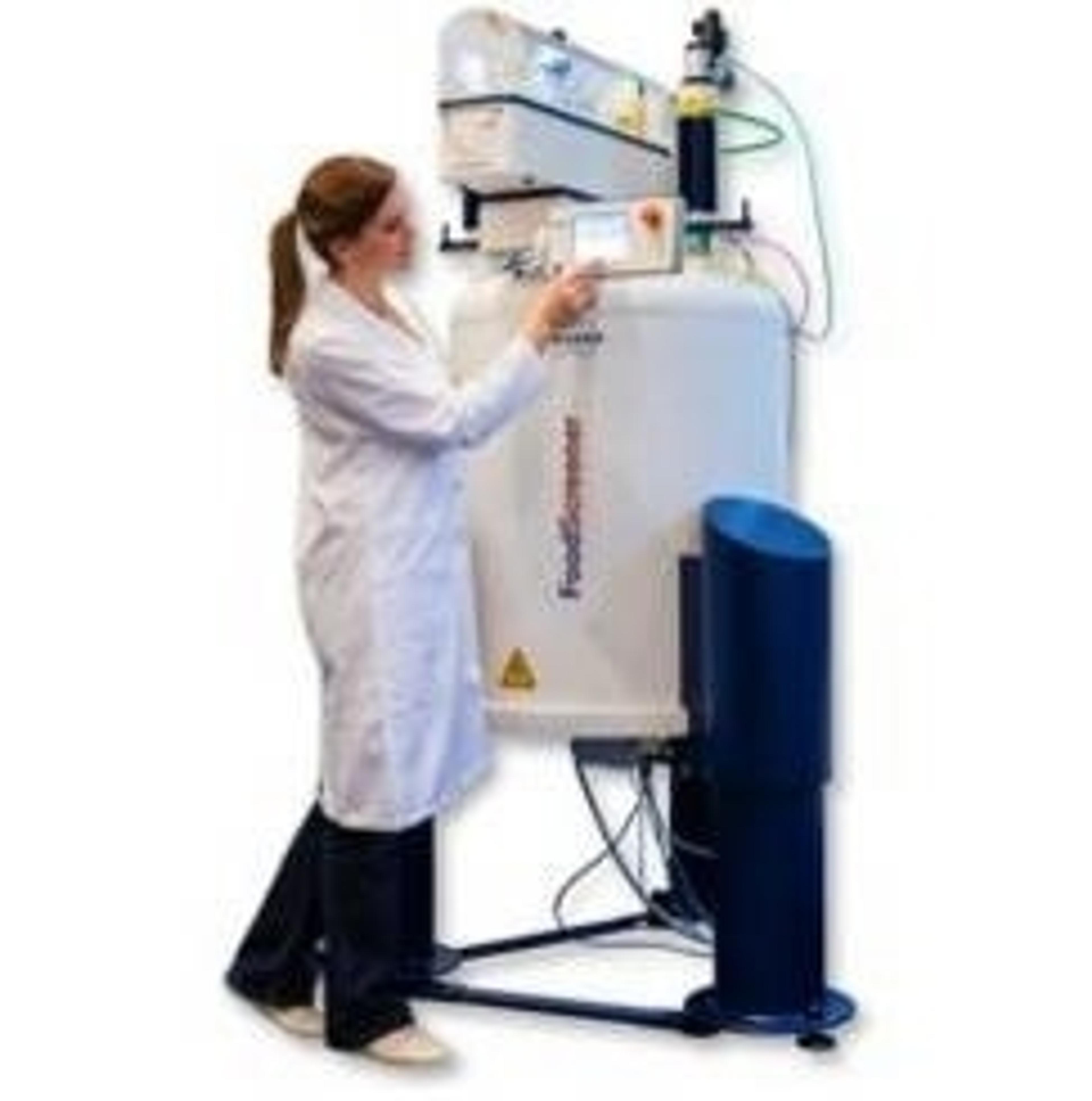
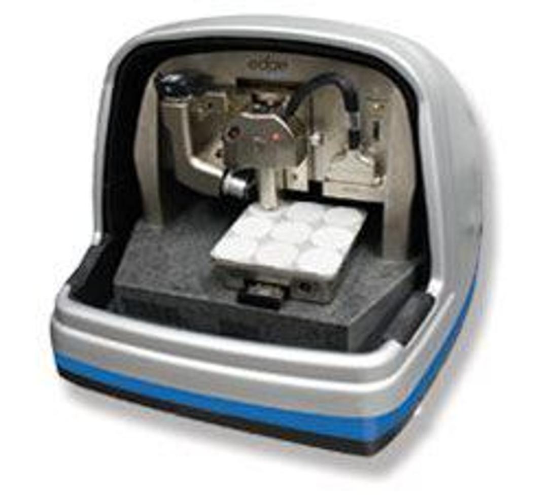
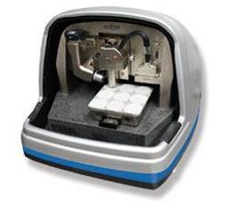
Dimension Edge™ AFM platform
Atomic Force Microscopy for Patterned Sapphire Substrates Delivering advanced automated metrology and production capabilities with superior resolution for now and the future. Bruker's Dimension Edge™ PSS Atomic Force Microscope with AutoMET™ Metrology Analysis Software is the ideal nano-metrology and nano-inspection system for LED substrate and epitaxial manufacturers. As an extension of the Dimension Edge AFM platform, the Ed…
The supplier does not provide quotations for this product through SelectScience. You can search for similar products in our Product Directory.
Reliable results, smart scanayst mode for scanning
Surface modification
This AFM is highly automated and reliable for a lot of surface analysis. We use it mostly for the roughness measurement. However, it did require a flat surface in order to have a relatively good image.
Review Date: 25 Feb 2016 | Bruker Nano Surfaces and Metrology
Atomic Force Microscopy for Patterned Sapphire Substrates
Delivering advanced automated metrology and production capabilities with superior resolution for now and the future.
Bruker's Dimension Edge™ PSS Atomic Force Microscope with AutoMET™ Metrology Analysis Software is the ideal nano-metrology and nano-inspection system for LED substrate and epitaxial manufacturers. As an extension of the Dimension Edge AFM platform, the Edge PSS incorporates the incredible value and resolution for which the Dimension AFM systems are renowned, while also providing a specialized solution for substrate measurements.
The system incorporates Bruker's proprietary AutoMET metrology analysis software, which has been designed specifically to meet the needs of patterned sapphire substrate (PSS) suppliers, providing a level of automation and ease of use never before seen in a value-price atomic force microscope.

Nanoscale mapping of permittivity and conductivity with scanning microwave impedance microscopy
Scanning microwave impedance microscopy (sMIM) is an atomic force microscopy (AFM)-based technique for materials and device characterization. The reflected microwave signal from the tip-sample interface holds information of the electrodynamic properties of the sample surface underneath the tip apex. In this application note from Bruker, explore sMIM and its integration with Bruker’s versatile AFM platforms, such as the Dimension Icon® and Dimension Edge™ AFMs. Furthermore, discover how when combined with Bruker’s exclusive PeakForce Tapping® mode, it is possible to obtain sMIM results on delicate samples, such as carbon nanotubes.
Deep learning to classify and establish structure property predictions with PeakForce QNM atomic force microscopy
Machine learning, is a powerful tool to establish the presence (or absence) of correlations between microstructure and bulk properties with its ability to flesh out relationships and trends that are difficult to establish otherwise. In this application note from Bruker, explore the use of deep learning tools, such as convolutional neural nets (CNNs), to explore atomic force microscopy (AFM) phase and PeakForce QNM® images of impact copolymers, a polymer blend of polypropylene with micro-sized domains of rubber.
Explore the Dimension Edge with ScanAsyst
In this application note, explore the Dimension Edge™ Atomic Force Microscope (AFM) which incorporates Bruker’s PeakForce Tapping® technology to provide the high levels of performance, functionality, and accessibility. Based on the Dimension Icon® platform, the Edge system has been designed from top to bottom to deliver the low drift and low noise necessary to achieve publication-ready data in minutes instead of hours, all at price points well below expectations for such performance. Furthermore, explore how ScanAsyst® imaging, integrated visual feedback, and preconfigured settings enable expert-level results simply and consistently.
Simultaneous electrical and mechanical property mapping at the nanoscale with PeakForce TUNA
Atomic force microscopy (AFM)-based conductivity measurements are a powerful technique for nanometer-scale electrical characterization on a wide range of samples. Tunneling AFM (TUNA), cover the lower current range (sub-pA up to nA). Bruker has developed an enhanced TUNA module with its proprietary PeakForce Tapping™ mode of operation that makes significant improvements to all three of these elements to enable exquisite tip-sample force control, quantitative nano-mechanical material property mapping through PeakForce QNM™, correlated nanoscale electrical property characterization through TUNA, and extreme ease of use through the ScanAsyst™ image optimization algorithms. A special probe has also been designed for use on particularly challenging samples. In this application note, explore the basics of PeakForce TUNA™, and compare it to standard Contact Mode–based TUNA.
Introduction to Bruker’s ScanAsyst and PeakForce Tapping AFM technology
PeakForce Tapping™ (PFT) and ScanAsyst™ (SA) are two atomic force microscope (AFM) imaging techniques that have been recently introduced by Bruker. In this application note, explore the underlying physical background, see how PFT fits into the framework of existing AFM modes, and discover the benefits of the new modes through application examples.