

Advances in microscopy for nanomaterial characterization
From high-resolution electron microscopy to chemical imaging and spectroscopy, explore the tools helping scientists reveal, characterize, and understand materials at the nanoscale.
How can researchers reveal structure, composition, and behavior at the nanoscale?
Advances in nanomaterials are driving innovation across electronics, energy storage, semiconductors and advanced manufacturing. Characterizing these increasingly complex materials requires powerful microscopy and analytical techniques capable of visualizing nanoscale features, identifying chemical composition, and uncovering structure-property relationships with greater precision.
Advances in electron microscopy (EM), infrared (IR) microscopy, Raman microscopy, and next-generation detector technologies are helping researchers answer some of the most challenging questions in materials science. Improved resolution, faster acquisition speeds, and richer datasets are revealing details that were previously hidden, from nanoscale structural changes and crystallographic features to the chemical composition of complex, multilayer materials.
In this SelectScience editorial feature, explore the technologies and workflows enabling deeper materials insight. Discover how researchers are using advanced EM and four-dimensional scanning transmission electron microscopy (4D-STEM) to generate high-resolution nanoscale data, how infrared and Raman microscopy can reveal the composition of multilayer materials, and how complementary analytical techniques support confident materials characterization and regulatory compliance.

Resource
A practical guide for understanding and testing hazardous substances in electrical and electronic products
Strengthen material characterization capabilities with guidance on analyzing hazardous substances, understanding regulatory requirements, and choosing the right analytical technologies for accurate, reliable results.
Download resource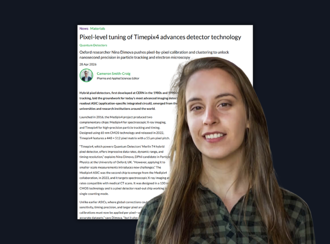
Article
Pixel-level tuning of Timepix4 advances detector technology
Discover how Oxford researcher Nina Dimova is pushing pixel-by-pixel calibration and clustering to unlock nanosecond precision in particle tracking and electron microscopy in this expert interview.
Read article
Webinar
Inside multilayer materials: Characterization by IR and Raman microscopy
In this webinar, Fabian Knechtel, Bruker Optics, will explore how IR and Raman microscopy and imaging can reveal the chemical composition and structure inside multilayer materials.
Register for free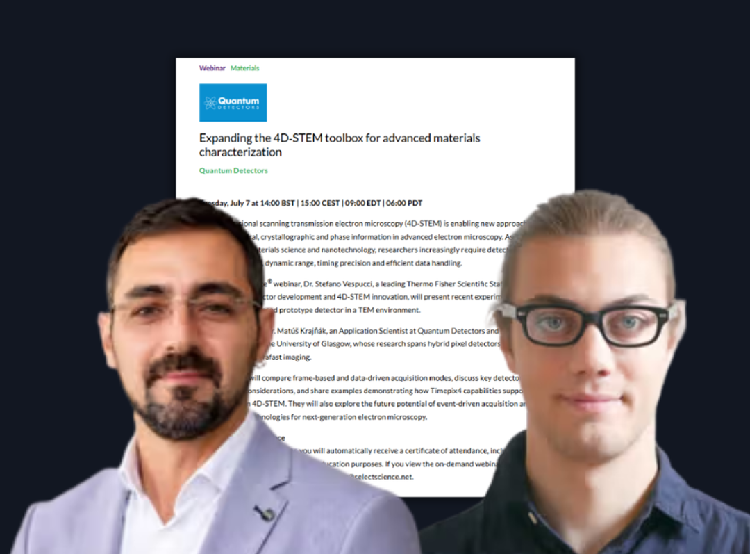
On-demand webinar
Expanding the 4D‑STEM toolbox for advanced materials characterization
Learn as experts compare frame‑based and data‑driven acquisition modes, discuss key detector performance considerations, and share examples demonstrating how Timepix4 capabilities support high‑resolution 4D‑STEM.
Watch now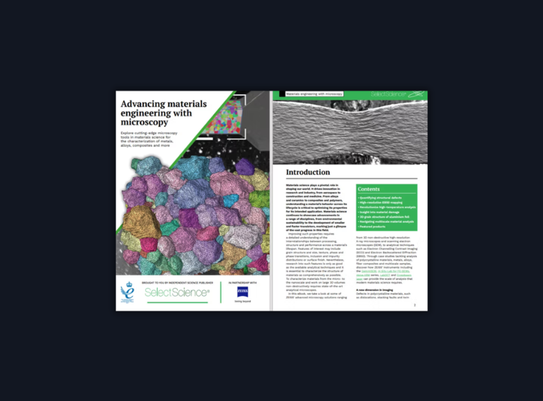
Application eBook
Advancing materials engineering with microscopy
Download this expert guide for free today and explore advanced microscopy solutions, including 3D non-destructive high-resolution X-ray microscopes and scanning electron microscopes (SEM).
Download eBook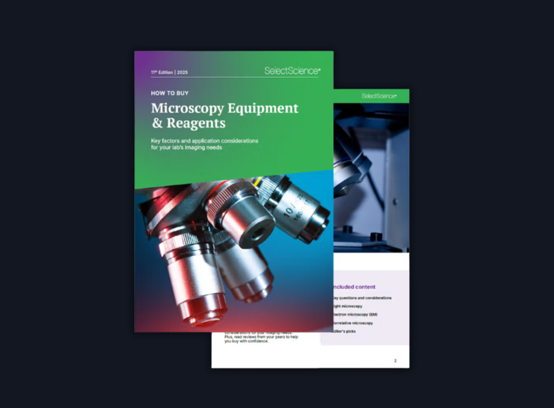
How-to-buy eBook
How to Buy Microscopy Equipment & Reagents
Learn about key factors and application considerations for your imaging needs. Plus, read reviews from your peers to help you buy with confidence.
Download eBook
Latest news & featured products

Never miss an update
Become a free SelectScience member and join our global scientific community to receive breaking news, expert interviews, and in‑depth insights straight to your inbox, along with regular newsletters covering key advances in microscopy for nanomaterial characterization.