Editorial ArticleMaterials
Atomic-scale imaging breaks speed barriers in Glasgow lab
Researchers harness next-generation detectors to capture magnetic dynamics in microseconds
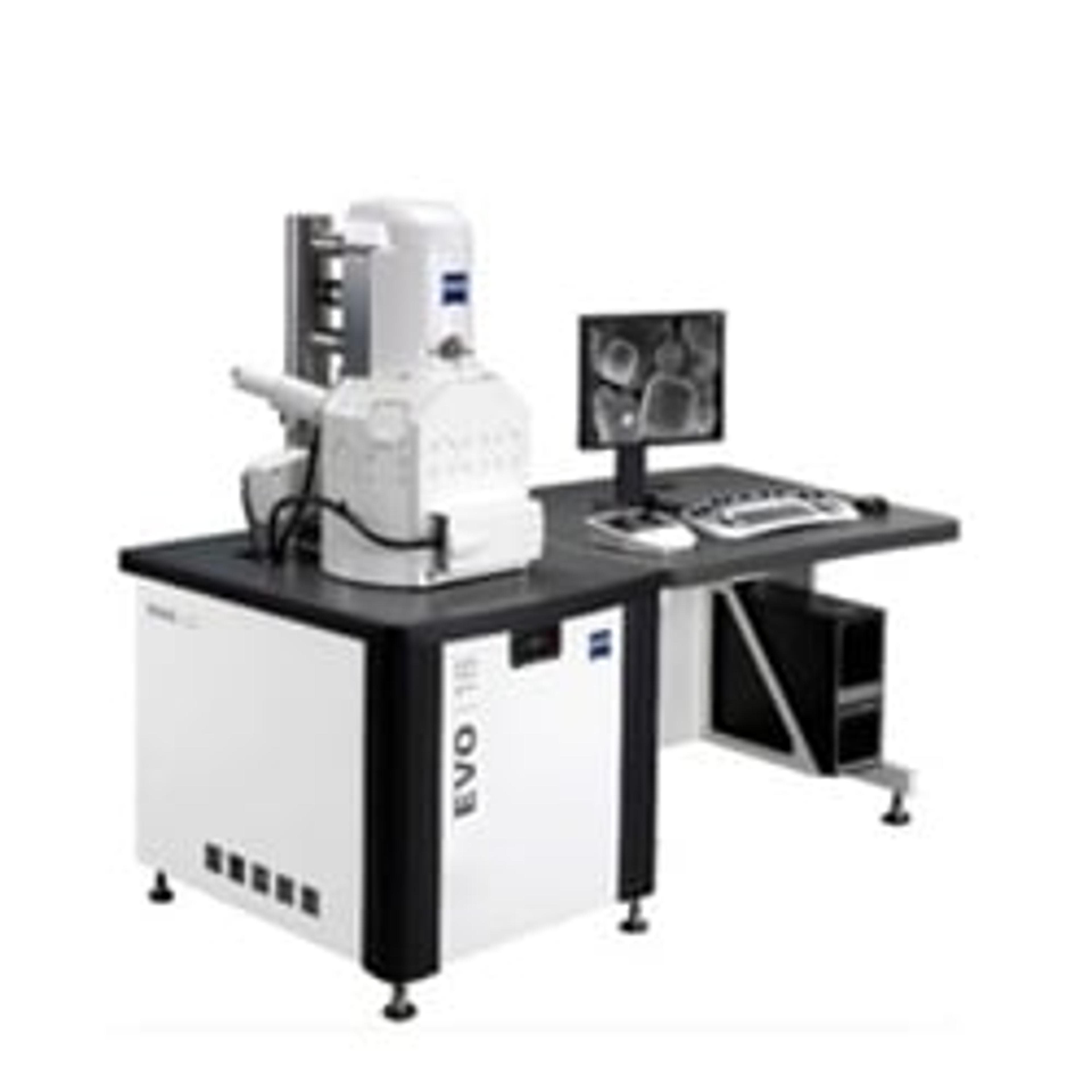
Scanning Electron Microscopy (SEM) is a technique that uses a focused electron beam to scan a sample and create high-resolution images. It is widely used in materials science, nanotechnology, and biological research. Explore SEM systems in our peer-reviewed product directory; compare products, check reviews, and get pricing directly from manufacturers.
Researchers harness next-generation detectors to capture magnetic dynamics in microseconds