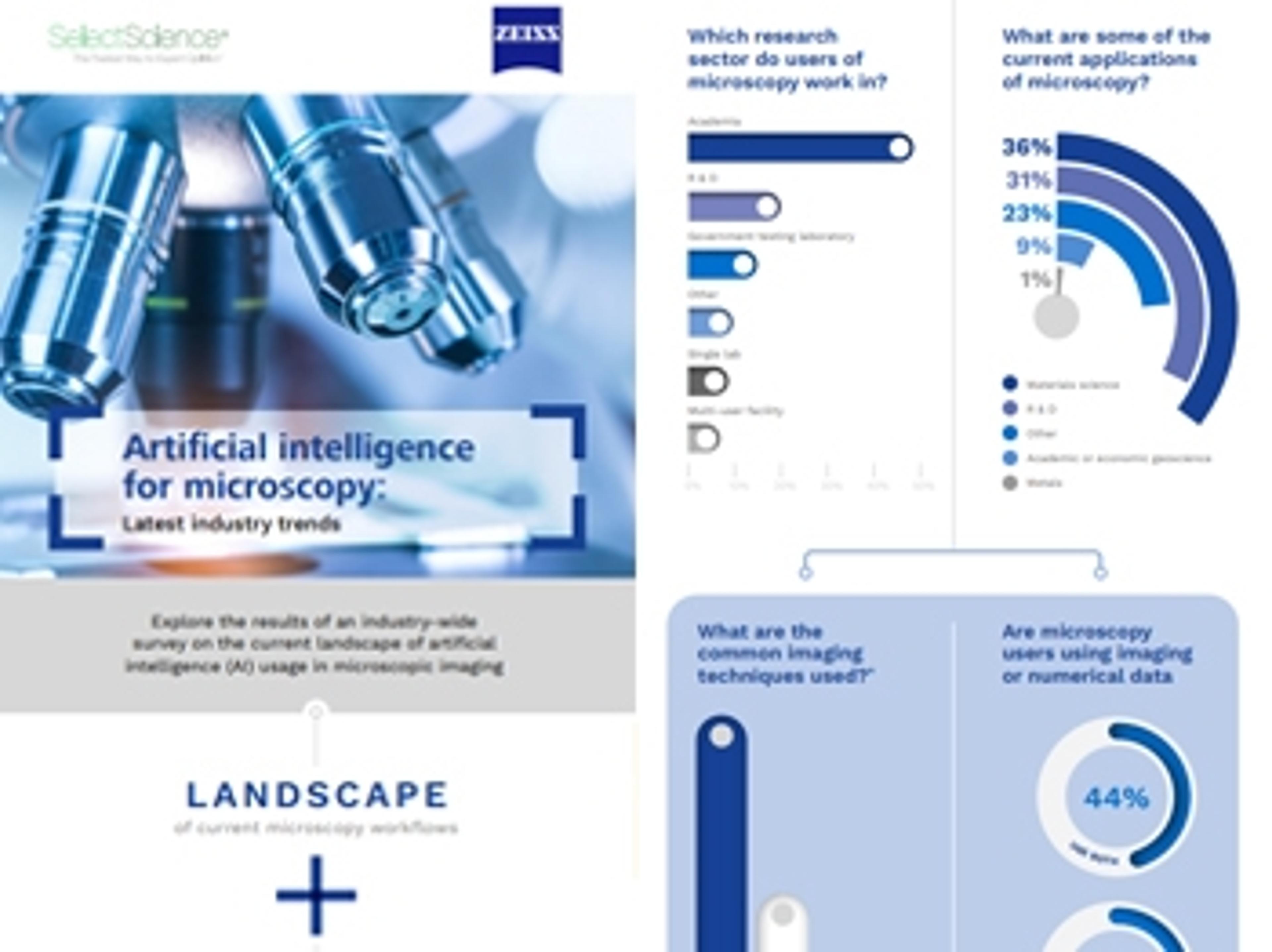
Resources
25
Selected Filters:

Application Note
Diffraction contrast tomography
Application Note
High-resolution imaging with ZEISS Gemini Optic on real samples
Application Note
Achieving nano-scaled EDS analysis in an SEM
Limitation and potential of STEM detector in SEM
Application Note
Principle setup of a ZEISS FIB-SEM
Exploring structure and functions of ZEISS FIB-SEM
Application Note
Rapid sample preparation for EBSD analysis
Advancements in microstructure preparation and materials characterization
Application Note
In situ SEM and Raman investigations on graphene
Comparison of graphene, graphene oxide and reduced graphene oxide
Application Note
Fabrication and characterization of nanofluidic devices for DNA optical mapping
Fast and flexible nanofluidic prototyping with FIB and SEM
Application Note
Voltage contrast in microelectronic engineering
Passive and active voltage contrast techniques for nanoscale circuit analysis
Application Note
Quantitative microstructural analysis of lithium-ion battery cathodes
Utilizing ZEISS ZEN Intellesis for enhanced insight
Application Note
Advanced FIB-SEM tomography for characterizing solid oxide electrolysis cells
Insights from ZEISS Atlas 5
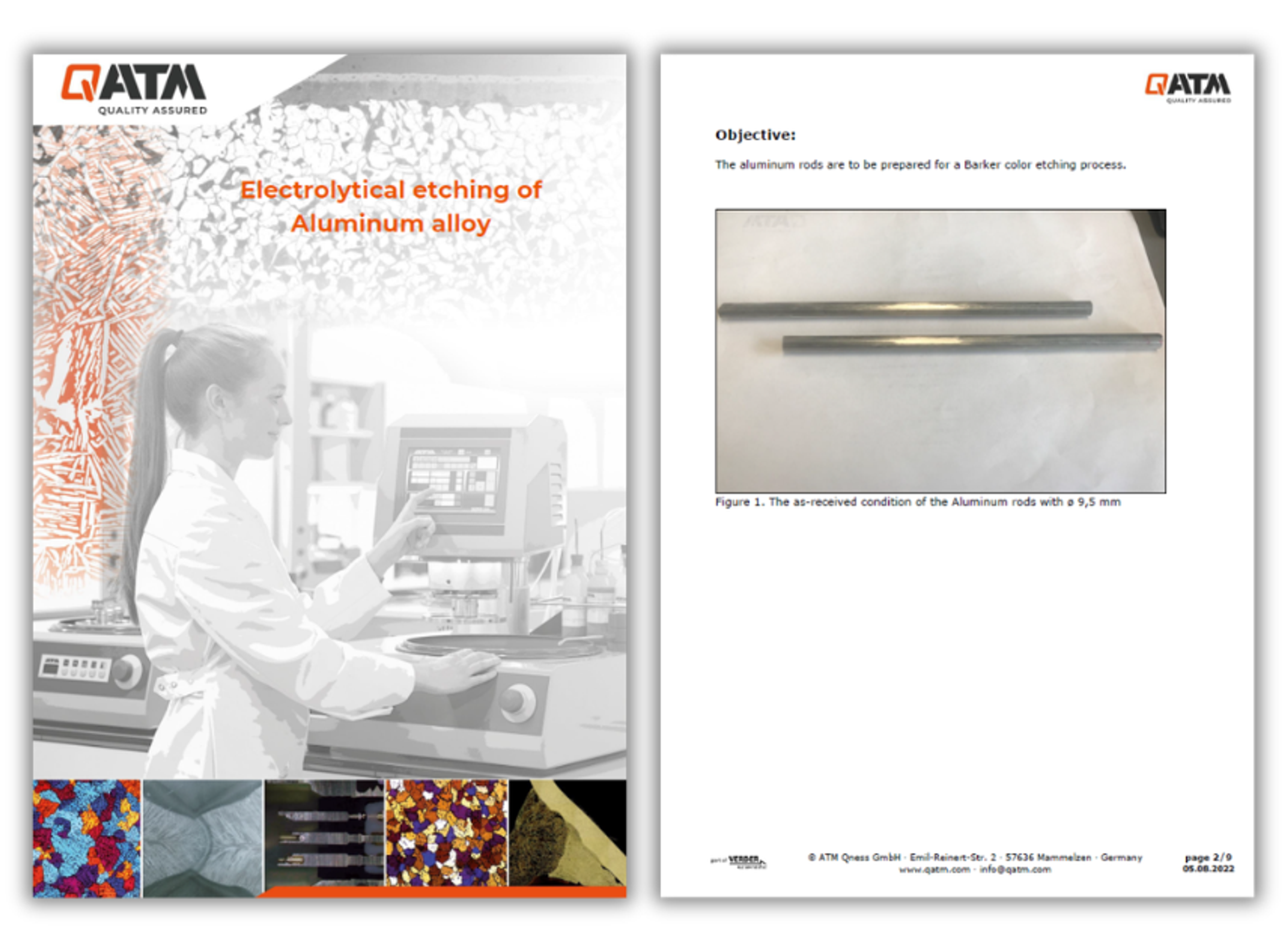
Application Note
Electrolytical etching of aluminum alloy
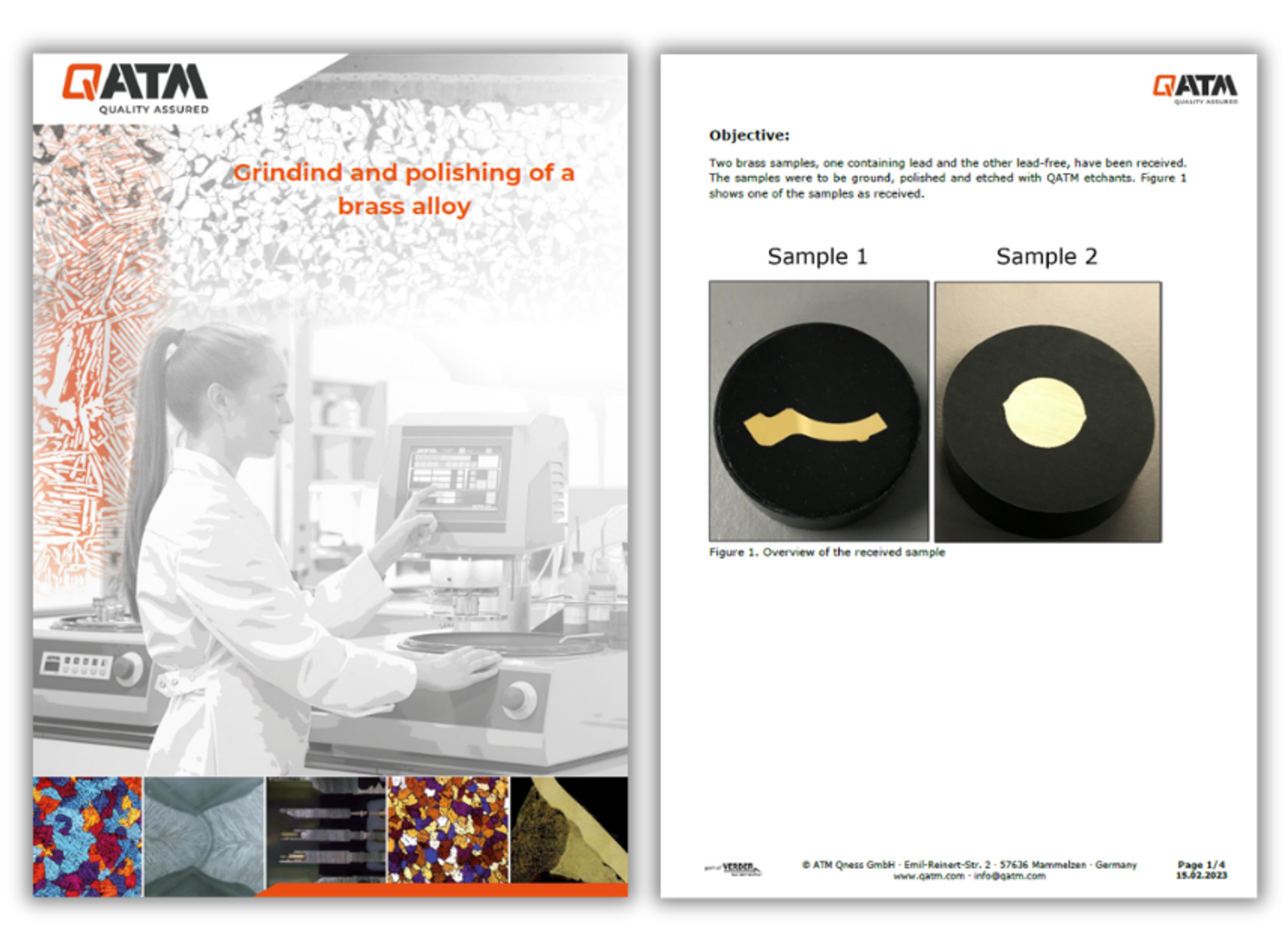
Application Note
Grinding and polishing of a brass alloy
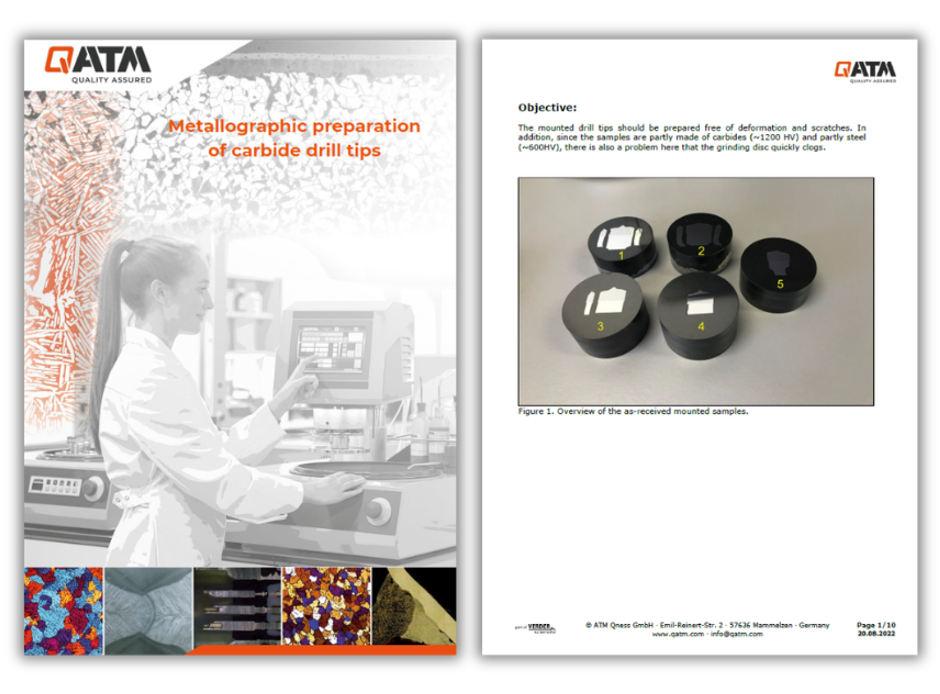
Application Note
Metallographic preparation of carbide drill tips
Application Note
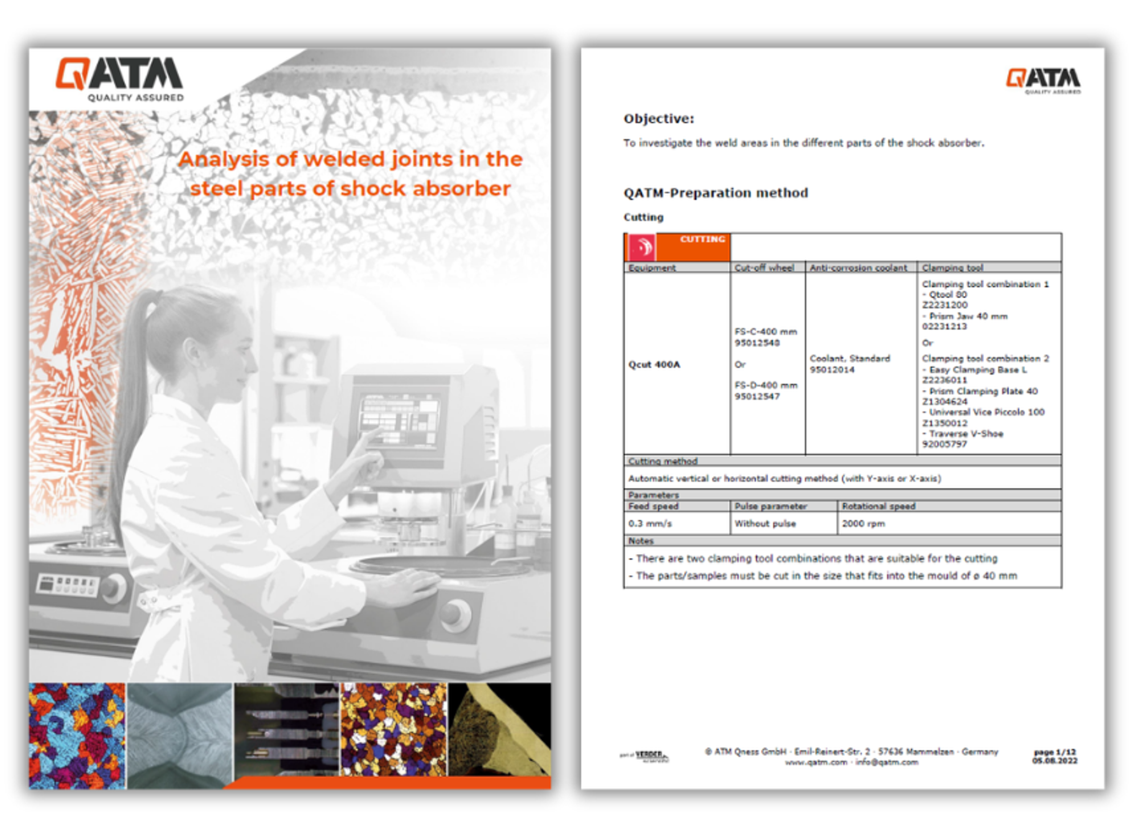
Analysis of welded joints in the steel parts of a shock absorber
Application Note
FE-SEM Imaging at 500V
Application Note
Supporting drug discovery with Amira Software
Product Brochures
Linking material properties to micro and nanostructures
Application Note
Particle size and shape analysis of powder coatings
Application Note