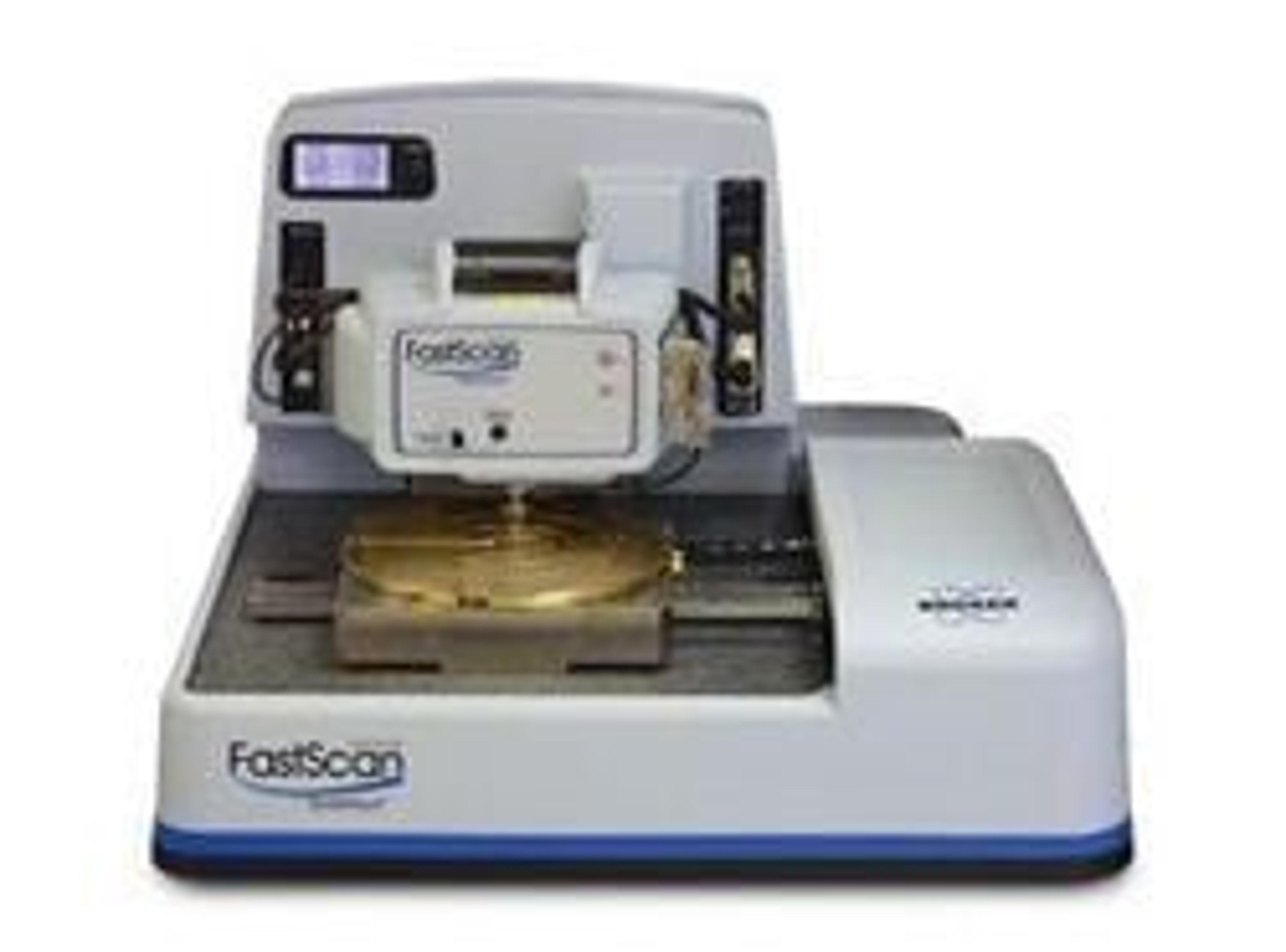
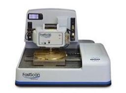
Dimension FastScan™
World's Ultimate AFM The new benchmark for speed with highest resolution and performanceThe Dimension FastScan™ delivers, for the first time, extreme imaging speed without loss of resolution, loss of force control, added complexity, or additional operating costs.This tip-scanning system provides measurements on both large and small size samples in air or fluids. With the FastScan you can achieve immediate atomic force microsc…


The supplier does not provide quotations for this product through SelectScience. You can search for similar products in our Product Directory.
Bruker FastScan is great for fast and reliable imaging.
Cellulose and protein characterization
Bruker FastScan is great for fast and reliable imaging.
Review Date: 21 Jun 2021 | Bruker Nano Surfaces and Metrology
World's Ultimate AFM
The new benchmark for speed with highest resolution and performance
The Dimension FastScan™ delivers, for the first time, extreme imaging speed without loss of resolution, loss of force control, added complexity, or additional operating costs.
This tip-scanning system provides measurements on both large and small size samples in air or fluids. With the FastScan you can achieve immediate atomic force microscopy images with the expected high resolution of a high-performance AFM, all in a single system. Whether surveying a sample scanning at >125Hz to find the region of interest, or scanning for detail at 1-second per image frame in air or fluids, the Dimension FastScan will redefine your AFM experience.
Dimension FastScan™ Features:
- Work hundreds of times faster with fast scanning rates up to frames per second, automated laser and detector alignment, comprehensive work flow and smart engaging
- Built-in measurement automation software in conjunction with higher speed ScanAsyst® provide exceptional measurement confidence and repeatability
- Precise force control at the tip renders high resolution and long tip-life
- Low-noise, temperature-compensated sensors in the scanners maintain sub-nanometer noise levels
- Closed-loop Icon and FastScan scanners keep vertical noise below 30pm and 40pm, respectively, as well as high accuracy with ultra-low drift
- Sample from subnanometer to hundreds of nanometers in height without loss of resolution

Improving the accuracy of nanomechanical measurements with force-curve-based AFM techniques
The structure and mechanical properties of sub-micron features in materials are of particular interest due to their influence on macroscopic material performance and function. Atomic force microscopy has the high resolution and force control to directly probe the mechanical properties of a wide range of these materials. In this application note from Bruker, consider the development and implementation of several new features that improve the flexibility, accuracy, and productivity of atomic force microscopes in measuring such important material properties as modulus and adhesion.
Performing hyperspectral mapping with AFM DataCube nanoelectrical modes
Atomic force microscopy (AFM)-based nanoelectrical modes have found applications in fields ranging from semiconductors to piezoelectric materials, energy research, and biology. Modes are available to characterize the local conductivity, resistivity, charge, carrier concentration, carrier-type, or piezoelectric properties with nanometer-scale spatial resolution, and usually require direct contact between the AFM tip and sample. In this application note, explore a new approach to nanoelectrical imaging that goes beyond a 2D map.
Measuring nanoscale viscoelastic properties with AFM-based nanoscale DMA
The development of heterogeneous materials like polymer composites, blends, and multilayers is of considerable importance in the chemicals industry. Bulk viscoelastic measurements are routine in establishing structure-property relationships for these materials. In this application note from Bruker, explore how the development of the AFM-nDMA™ mode, can avoid issues associated with measuring nanoscale viscoelastic properties and how the frequency and temperature dependence of viscoelastic properties in rheologically relevant ranges can be directly measured with 10 nm spatial resolution.
Deep learning to classify and establish structure property predictions with PeakForce QNM atomic force microscopy
Machine learning, is a powerful tool to establish the presence (or absence) of correlations between microstructure and bulk properties with its ability to flesh out relationships and trends that are difficult to establish otherwise. In this application note from Bruker, explore the use of deep learning tools, such as convolutional neural nets (CNNs), to explore atomic force microscopy (AFM) phase and PeakForce QNM® images of impact copolymers, a polymer blend of polypropylene with micro-sized domains of rubber.
Explore the Bruker Dimension FastScan
In this application note, explore the Dimension FastScan® Atomic Force Microscope (AFM) which delivers extreme imaging speed without sacrificing the Dimension Icon® resolution and performance.
Quantitative mechanical property mapping at the nanoscale with PeakForce QNM
The scanning probe microscope (SPM) has long been recognized as a useful tool for measuring the mechanical properties of materials. Until recently though, it has been impossible to achieve truly quantitative material property mapping with the resolution and convenience demanded by SPM researchers. A number of recent SPM mode innovations have taken aim at these limitations, and now, with Bruker’s PeakForce QNM®, it is possible to identify material variations unambiguously and at high resolution across a topographic image. In this application note, explore the principles and benefits of the PeakForce QNM imaging mode.
Simultaneous electrical and mechanical property mapping at the nanoscale with PeakForce TUNA
Atomic force microscopy (AFM)-based conductivity measurements are a powerful technique for nanometer-scale electrical characterization on a wide range of samples. Tunneling AFM (TUNA), cover the lower current range (sub-pA up to nA). Bruker has developed an enhanced TUNA module with its proprietary PeakForce Tapping™ mode of operation that makes significant improvements to all three of these elements to enable exquisite tip-sample force control, quantitative nano-mechanical material property mapping through PeakForce QNM™, correlated nanoscale electrical property characterization through TUNA, and extreme ease of use through the ScanAsyst™ image optimization algorithms. A special probe has also been designed for use on particularly challenging samples. In this application note, explore the basics of PeakForce TUNA™, and compare it to standard Contact Mode–based TUNA.
Introduction to Bruker’s ScanAsyst and PeakForce Tapping AFM technology
PeakForce Tapping™ (PFT) and ScanAsyst™ (SA) are two atomic force microscope (AFM) imaging techniques that have been recently introduced by Bruker. In this application note, explore the underlying physical background, see how PFT fits into the framework of existing AFM modes, and discover the benefits of the new modes through application examples.
PeakForce Kelvin probe force microscopy
Kelvin probe force microscopy (KPFM), also called surface potential microscopy, has found broad applications, ranging from corrosion studies of alloys, photovoltaic effects on solar cells, and surface analysis. KPFM, together with conductive atomic force microscopy (AFM), has been recognized as the two most used nanoscale electrical characterization tools, complementing each other. In this application note from Bruker, explore how limited spatial resolution and lack of measurement repeatability and accuracy have limited KPFMs usefulness in some critical areas, such as in the identification of donor and acceptor domains in bulk heterojunction organic solar cells, material differentiation in composite materials, and trapped charges on insulators.
Toward Quantitative Nanomechanical Measurements on Live Cells with PeakForce QNM
This application note reviews recent progress in mapping the properties of soft samples such as cells and gels with force volume and PeakForce QNM and the use of the newest NanoScopeR and NanoScope Analysis features to collect and analyze the data from these techniques.
Study Biological Dynamics with the New Dimension FastScan From Bruker
In this video Andrea Slade, an Applications Specialist at Bruker-Nano, tells SelectScience how the new Dimension FastScan is helping researchers to overcome the current limitations associated with Atomic Force Microscopy (AFM). With this new technology researches can now study biological dynamics, for example cell migration. As its name suggests the Dimension FastScan enables faster scanning, which not only results in high spatial resolution, but also in high temporal resolution. Interview filmed by SelectScience at ASCB 2012.

Advancements in materials characterization: From decoding polymers and battery materials to harnessing the power of atomic force microscopy
Explore advanced technologies and the latest resources to support your materials characterization