Performing hyperspectral mapping with AFM DataCube nanoelectrical modes
22 Jun 2023Atomic force microscopy (AFM)-based nanoelectrical modes have found applications in fields ranging from semiconductors to piezoelectric materials, energy research, and biology. Modes are available to characterize the local conductivity, resistivity, charge, carrier concentration, carrier-type, or piezoelectric properties with nanometer-scale spatial resolution, and usually require direct contact between the AFM tip and sample. In this application note, explore a new approach to nanoelectrical imaging that goes beyond a 2D map.
Related products
Request Quote for All Products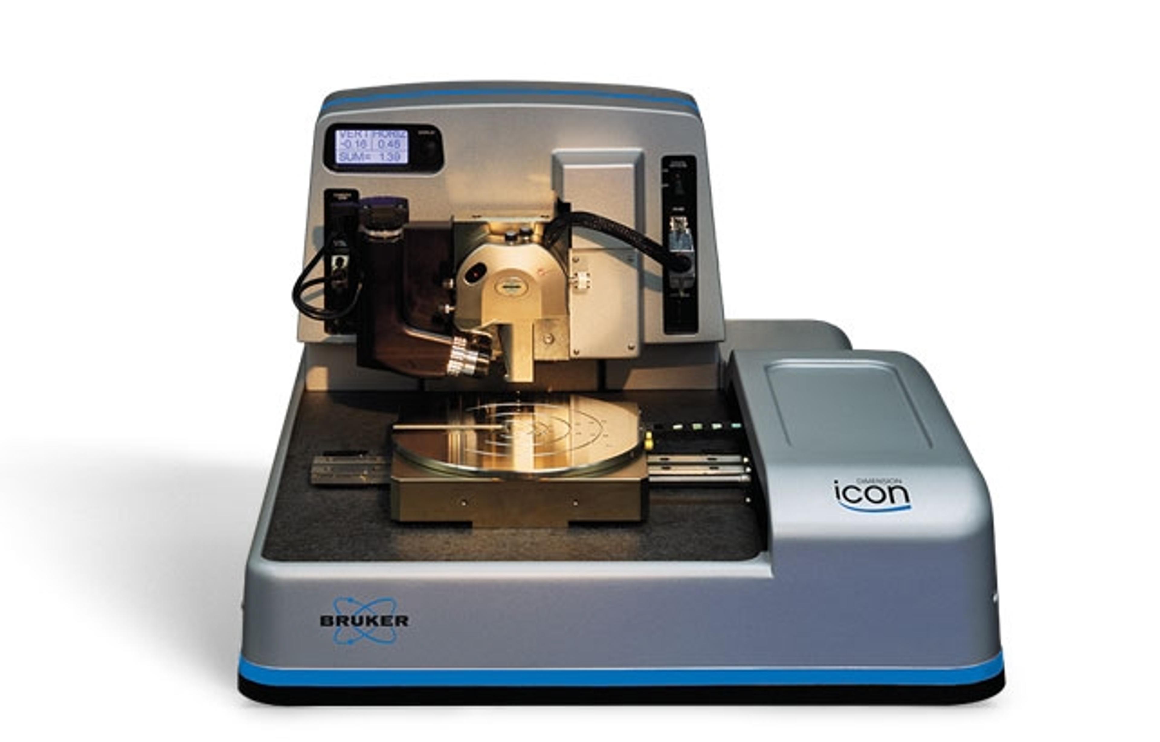
Dimension Icon
Bruker Nano Surfaces and MetrologyBruker’s Dimension Icon brings the highest levels of performance, functionality, and AFM accessibility to nanoscale researchers in science and industry. Building upon the world’s most utilized large-sample AFM platform, it is the culmination of decades of technological innovation, customer feedback, and industry-leading application flexibility.
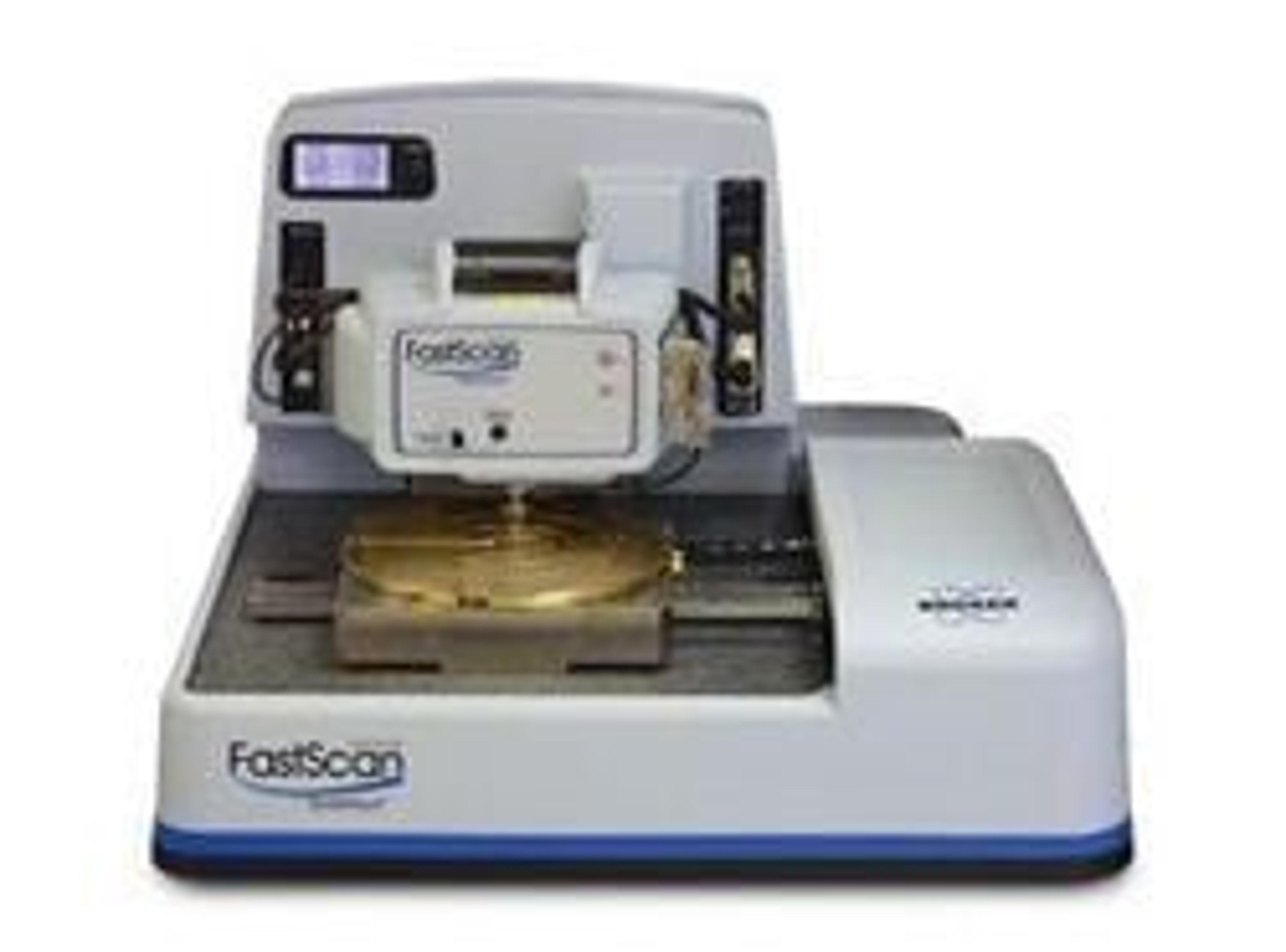
Dimension FastScan™
Bruker Nano Surfaces and MetrologyWorld's Ultimate AFM The new benchmark for speed with highest resolution and performanceThe Dimension FastScan™ delivers, for the first time, extreme imaging speed without loss of resolution, loss of force control, added complexity, or additional operating costs.This tip-scanning system provides measurements on both large and small size samples in air or fluids. With the FastScan you can achieve immediate atomic force microscopy images with the expected high resolution of a high-performance AFM, all in a single system. Whether surveying a sample scanning at >125Hz to find the region of interest, or scanning for detail at 1-second per image frame in air or fluids, the Dimension FastScan will redefine your AFM experience.Dimension FastScan™ Features: Work hundreds of times faster with fast scanning rates up to frames per second, automated laser and detector alignment, comprehensive work flow and smart engaging Built-in measurement automation software in conjunction with higher speed ScanAsyst® provide exceptional measurement confidence and repeatability Precise force control at the tip renders high resolution and long tip-life Low-noise, temperature-compensated sensors in the scanners maintain sub-nanometer noise levels Closed-loop Icon and FastScan scanners keep vertical noise below 30pm and 40pm, respectively, as well as high accuracy with ultra-low drift Sample from subnanometer to hundreds of nanometers in height without loss of resolution