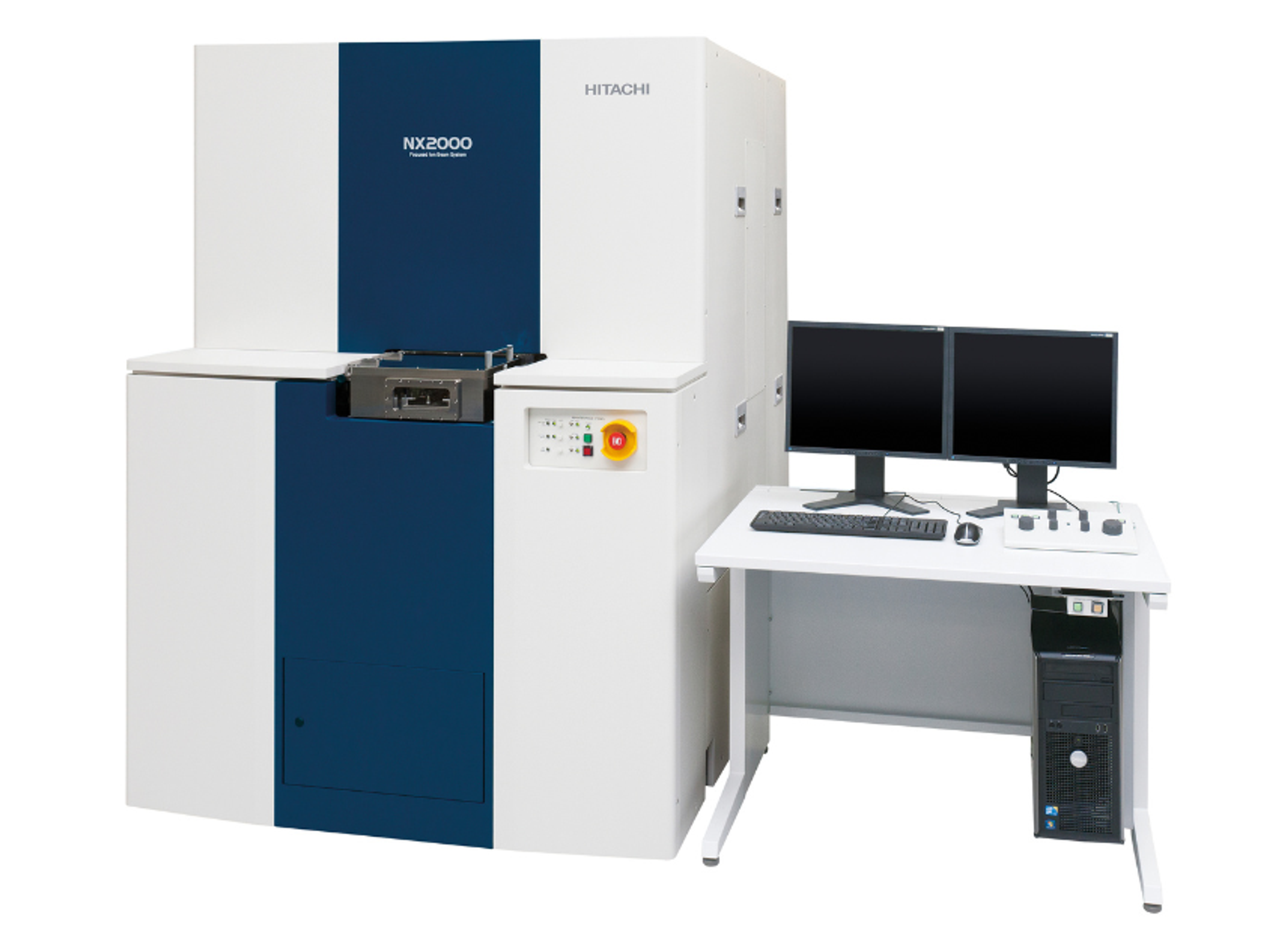
NX2000
FIB-SEM for the semiconductor sector with 200mm wafer coverage


The supplier does not provide quotations for this product through SelectScience. You can search for similar products in our Product Directory.
NX2000 is a FIB-SEM optimised for semiconductor applications (defect analysis with KLARF coordinate import, TEM lamella extraction, device development). With 205 x 205 mm X,Y travel, the sample stage even allows full-surface processing of 200 mm wafers without sample rotation. The vertically mounted Ga FIB allows up to 100nA ion current at 30 kV. The FE-SEM column is equipped with a cold field emitter.
Brochures

Hitachi Product Catalogue 2024/25- German
In this brochure, Hitachi High-Technologies present a wide range of electron microscopes and ion beam systems available, organised by product class, in German. Each tool is designed to reliably meet your application needs.
Hitachi Product Catalogue 2024/25- English
In this brochure, Hitachi High-Technologies present a wide range of electron microscopes and ion beam systems available, organised by product class. Each tool is designed to reliably meet your application needs.