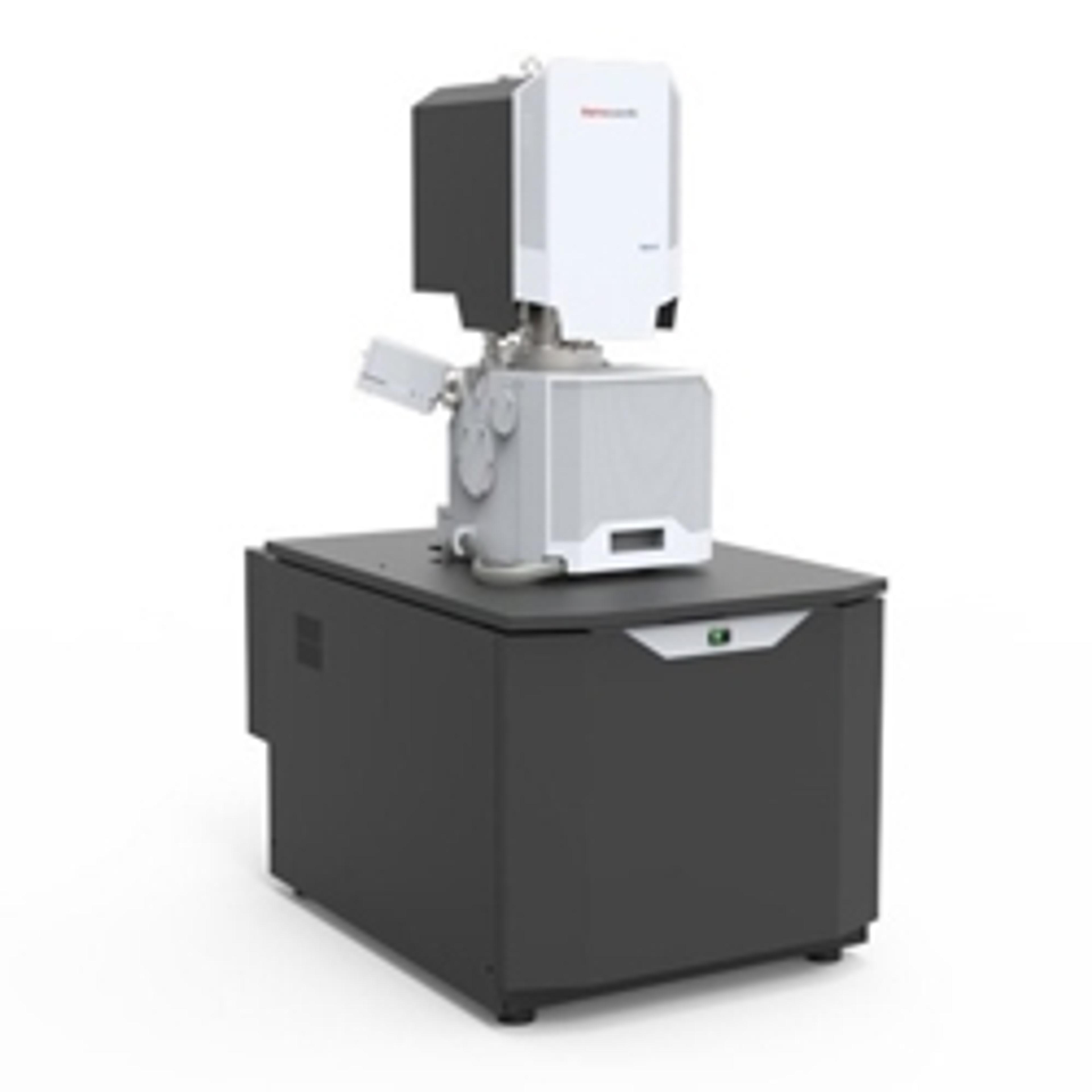
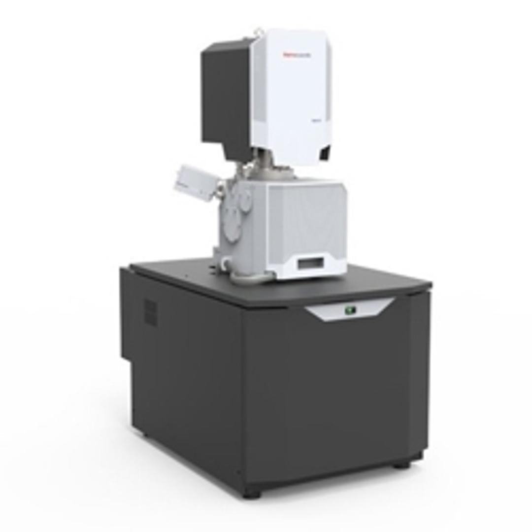
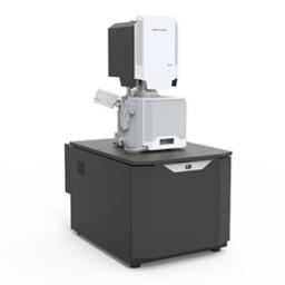
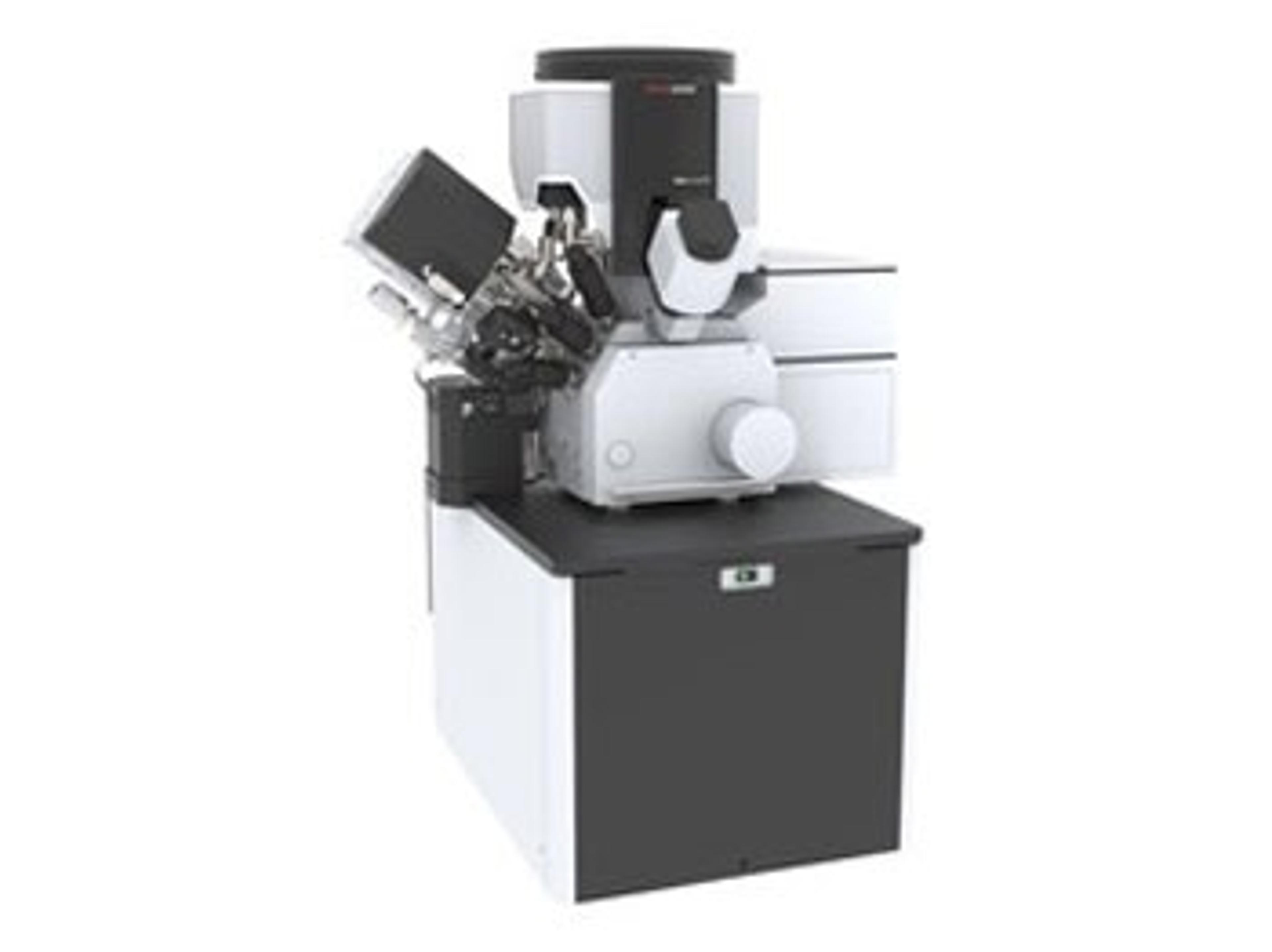
Apreo™ SEM for Materials Science
The most versatile high-performance SEM.

The supplier does not provide quotations for this product through SelectScience. You can search for similar products in our Product Directory.
Great results.
Nanoparticles
Easy to use and has many functions such as EDX.
Review Date: 18 Nov 2022 | Thermo Fisher Scientific
Great instrument, improves my research a lot.
Analyze nanoparticles on glass substrate
it is fast and user friendly. I like to use it. Preparing my sample on glass substrate make my research easier!
Review Date: 15 Nov 2019 | Thermo Fisher Scientific
The most versatile high-performance SEM. The Thermo Scientific™ Apreo scanning electron microscope's (SEM) revolutionary compound lens design combines electrostatic and magnetic immersion technology to yield unprecedented resolution and signal selection. This makes the Apreo SEM the platform of choice for research on nanoparticles, catalysts, powders and nanodevices, without compromising on magnetic sample performance. The Apreo SEM benefits from the unique in-lens backscatter detection, which provides excellent materials contrast, even at tilt, short working distance, or on sensitive samples. The novel compound lens further improves contrast with energy filtering and adds charge filtering for imaging of insulating samples. The optional low vacuum mode now has a 500 Pa maximum chamber pressure for imaging even the most demanding insulators. With all these options, including the compound final lens, advanced detection and flexible sample handling, the Apreo SEM's performance and versatility will meet your research challenges for many years to come.
Experience the advantages of the Apreo SEM:
- The unique compound final lens delivers an exceptional resolution of 1.0 nm at 1 kV, without the need for beam deceleration - on any sample, even if it is tilted or topographic.
- The most useful backscatter detection - materials contrast is always available, even at low voltage and beam currents, at any tilt angle, on beam sensitive samples and at TV-rate imaging.
- Unparalleled detector flexibility - obtain the contrast or signal intensity that matters most by combining information from individual detector segments.
- The widest range of charge mitigation strategies , including a low vacuum mode with a chamber pressure of up to 500 Pa to enable imaging of any sample.
- A superior analytics platform provided by high beam currents and a small spotsize. The chamber supports three EDS detectors, coplanar EDS & EBSD, and low vacuum optimized for analytics.
- Easiest sample handling and navigation with the multi-purpose sample holder and the Nav-Cam+.
- Expert results for new users through advanced user guidance, presets and undo functionality.

SEM and EDS analysis in industry
As the complexity of industrial processes increases, so does the need for more rigorous, high-quality analysis to ensure that products meet all standards of quality and reliability. Scanning electron microscopy (SEM) has become a common tool for modern research and development, as well as for failure analysis and troubleshooting, because it provides detailed (nanometer-scale) information about the surface structure of samples. SEM is often used in conjunction with energy dispersive X-ray spectroscopy (EDS), which adds elemental information to the surface imaging data.
Download this ebook to learn more about:
- How the joint application of SEM and EDS analysis supports in-depth material characterization for industrial applications
- How Thermo Scientific ColorSEM Technology is designed to integrate these two techniques into a single, fast, easy-to-use package, accessible to novices and experts alike
An introduction to elemental analysis with ColorSEM Technology
Elemental analysis with traditional EDS (energy dispersive X-ray spectroscopy) runs on a dedicated hardware and software system. This requires constant switching between two separate operating platforms, usually navigating through complex workflows to get to the answer. In this application note, discover how the Thermo Scientific™ ColorSEM™ Technology can overcome this, delivering new levels of speed, convenience, and insight during SEM EDS analysis. Download it below to learn more about:
- The X-rays collection process
- Spectral processing steps
- Modes of analysis
- ColorSEM technology applications
Helios 5 Laser PFIB accelerates the pace of materials research for academic and industrial users
First-of-its-kind commercial solution analyzes 3D and sub-surface data 15,000 times faster than a typical Ga-FIB