ResourceLife Sciences
ZEISS Gemini Optics: High-Resolution Images with Real-World Samples
22 Jul 2018In this poster, ZEISS demonstrates the capacity of Gemini Optics with a variety of real-world samples, ranging from metal particles to biological materials.
Related products
Request Quote for All Products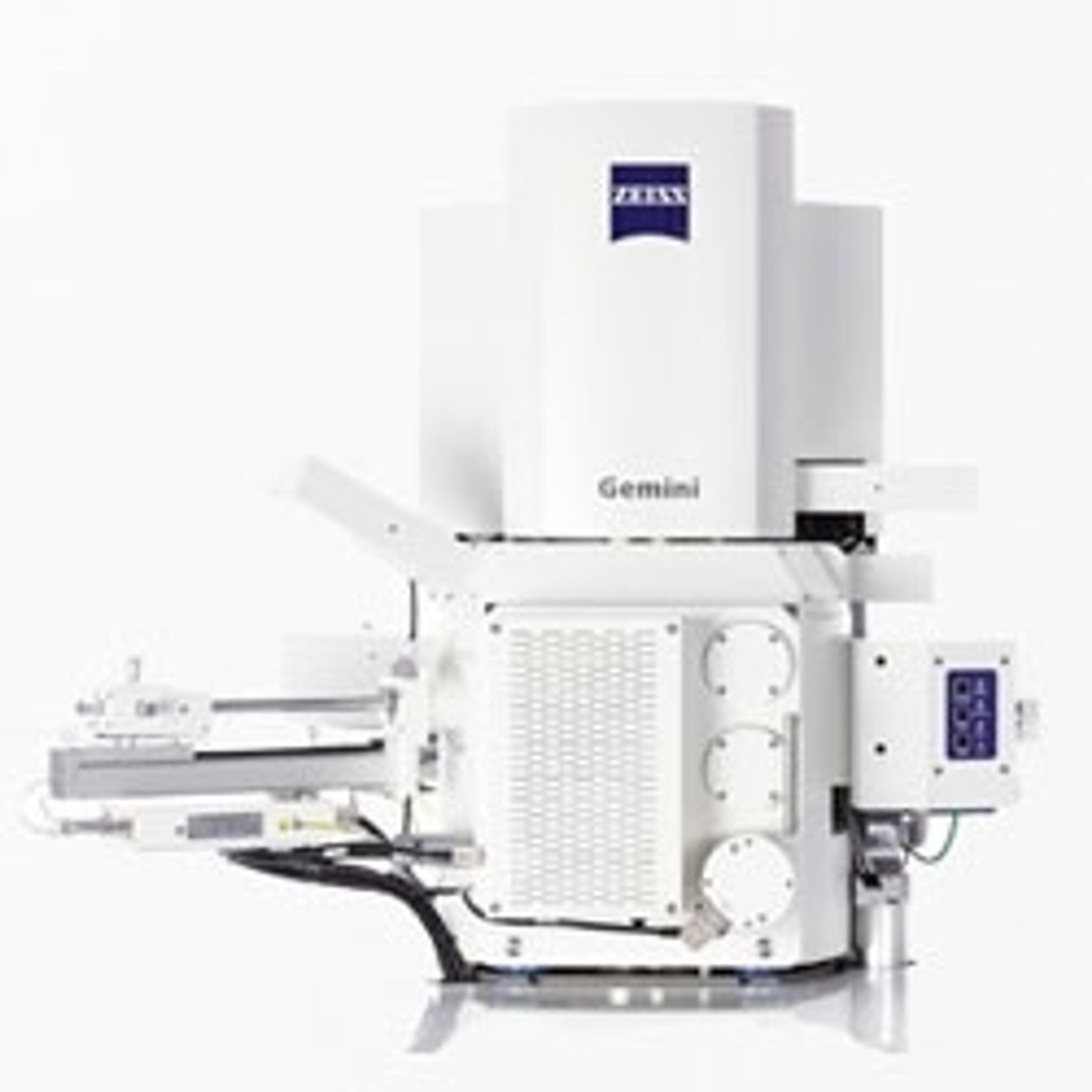
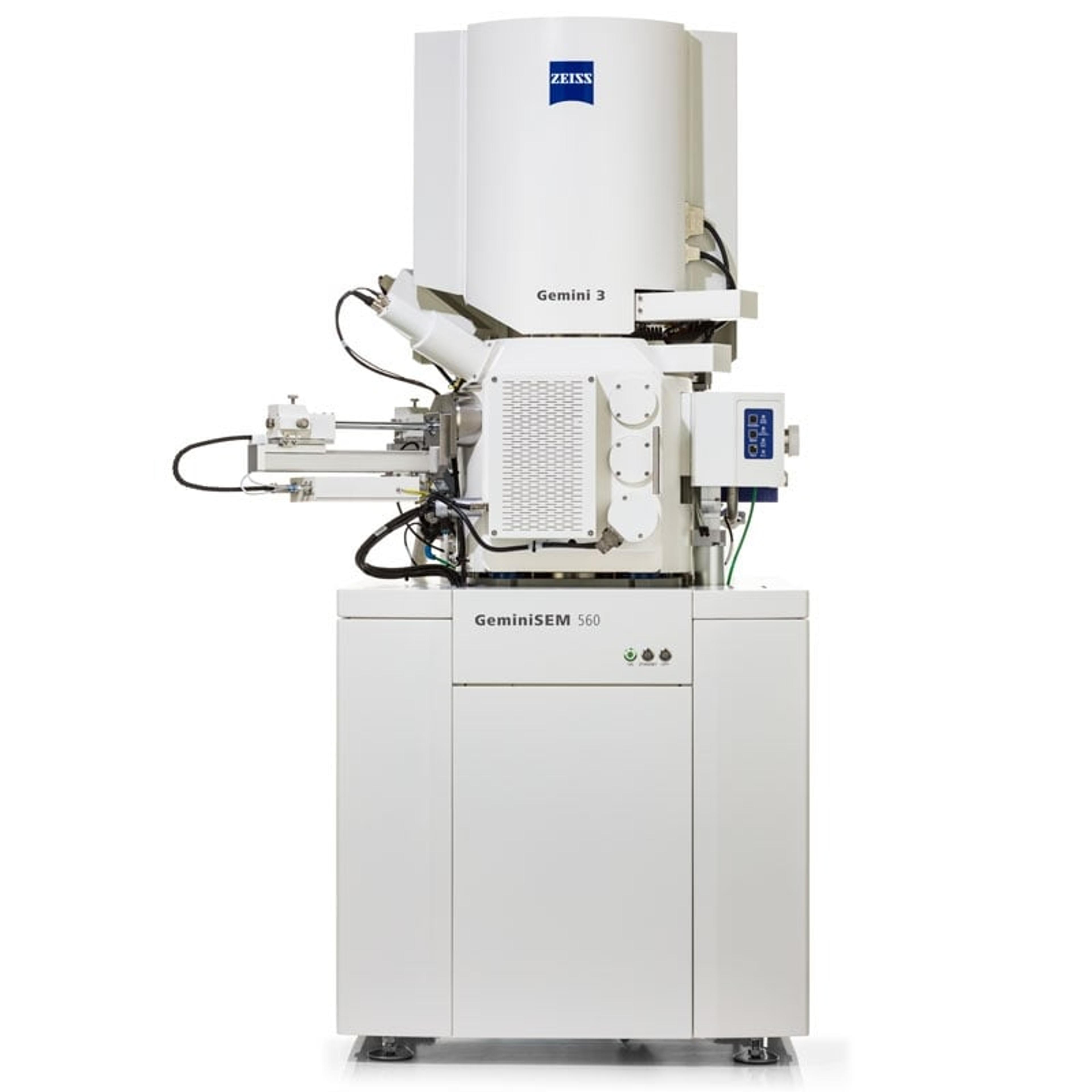
ZEISS GeminiSEM for Life Sciences
ZEISS Research Microscopy SolutionsFor the Highest Demands in Imaging and Analytics from Any Sample
ZEISS GeminiSEM Family
ZEISS Research Microscopy SolutionsFor Your Highest Demands in Sub-nanometer Imaging, Analytics and Sample Flexibility
Links
Tags
Electron MicroscopyElectron microscopes (EM) are used to create high-resolution images of samples at the nanoscale by means of an accelerated beam of electrons as a source of illumination. Types of electron microscope include scanning electron microscopes (SEM), transmission electron microscopes (TEM), scanning transmission electron microscopes (STEM) and cryo-electron microscopes. Focused ion beam (FIB) microscopes are useful for modifying or milling a sample surface with nanometer precision, as well as imaging. Find the best electron microscopes in our peer-reviewed product directory: compare products, check customer reviews and receive pricing direct from manufacturers.Molecular BiologyMolecular biology is the branch of biology that focuses on the molecular mechanisms that underlie cellular functions. It involves studying DNA, RNA, and proteins to understand gene expression, replication, and regulation. Molecular biology is fundamental to biotechnology, medicine, and genetic research. Explore molecular biology products in our peer-reviewed product directory; compare products, check reviews, and get pricing directly from manufacturers.High Content ImagingHigh content imaging is a method combining two or more fluorescent microscopy experiments to identify substances that alter a cell’s phenotype in a desired manner. The process is adapted to multi-well plates and both the image acquisition and analysis are automated.Super Resolution MicroscopyNanomaterialsNanomaterials such as carbon nanotubes, fullerenes and nanoparticles are a group of materials that measure between 1-1000nm for a single unit. Analysis techniques include AFM, electron microscopy and super resolution microscopy.SEMScanning Electron Microscopy (SEM) is a technique that uses a focused electron beam to scan a sample and create high-resolution images. It is widely used in materials science, nanotechnology, and biological research. Explore SEM systems in our peer-reviewed product directory; compare products, check reviews, and get pricing directly from manufacturers.