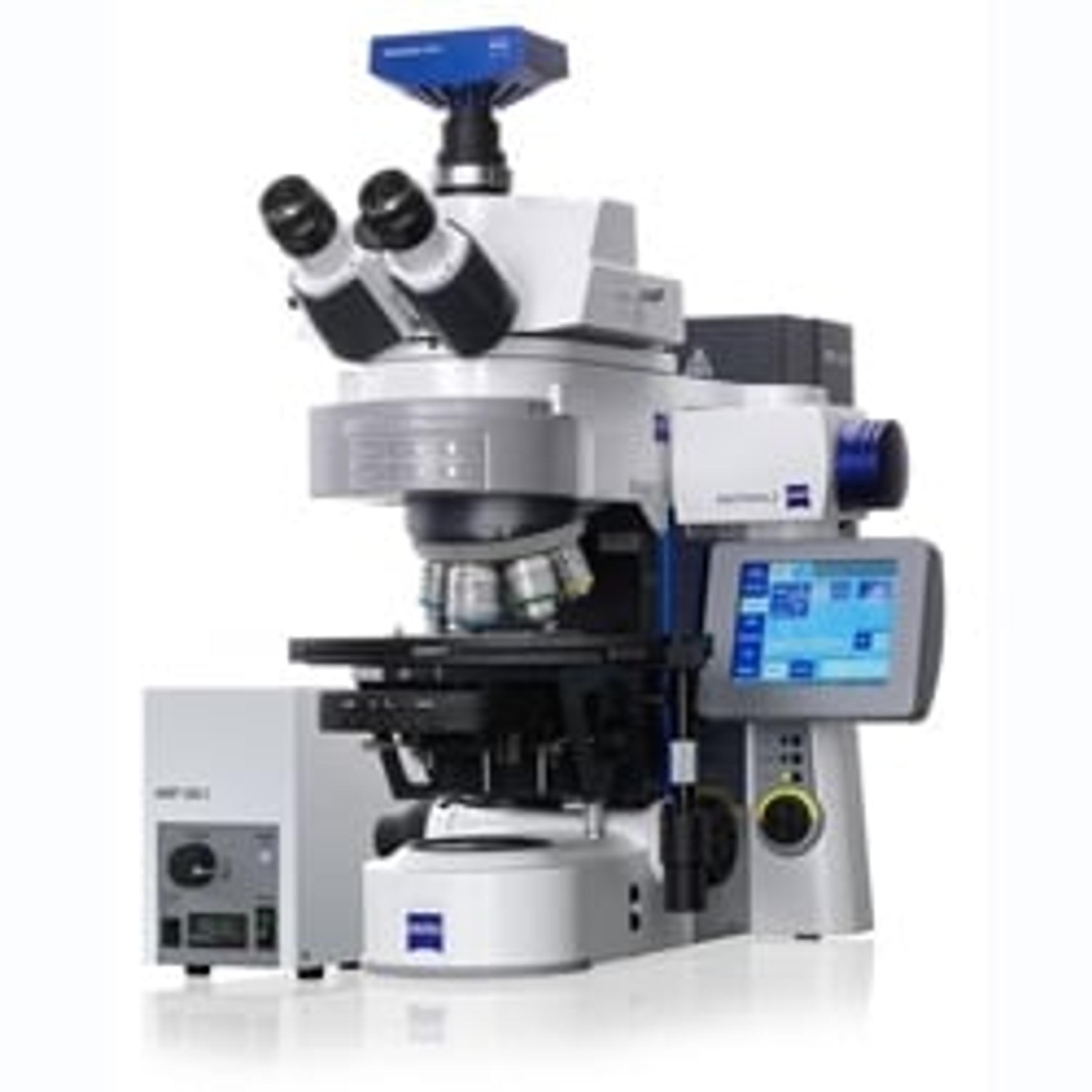
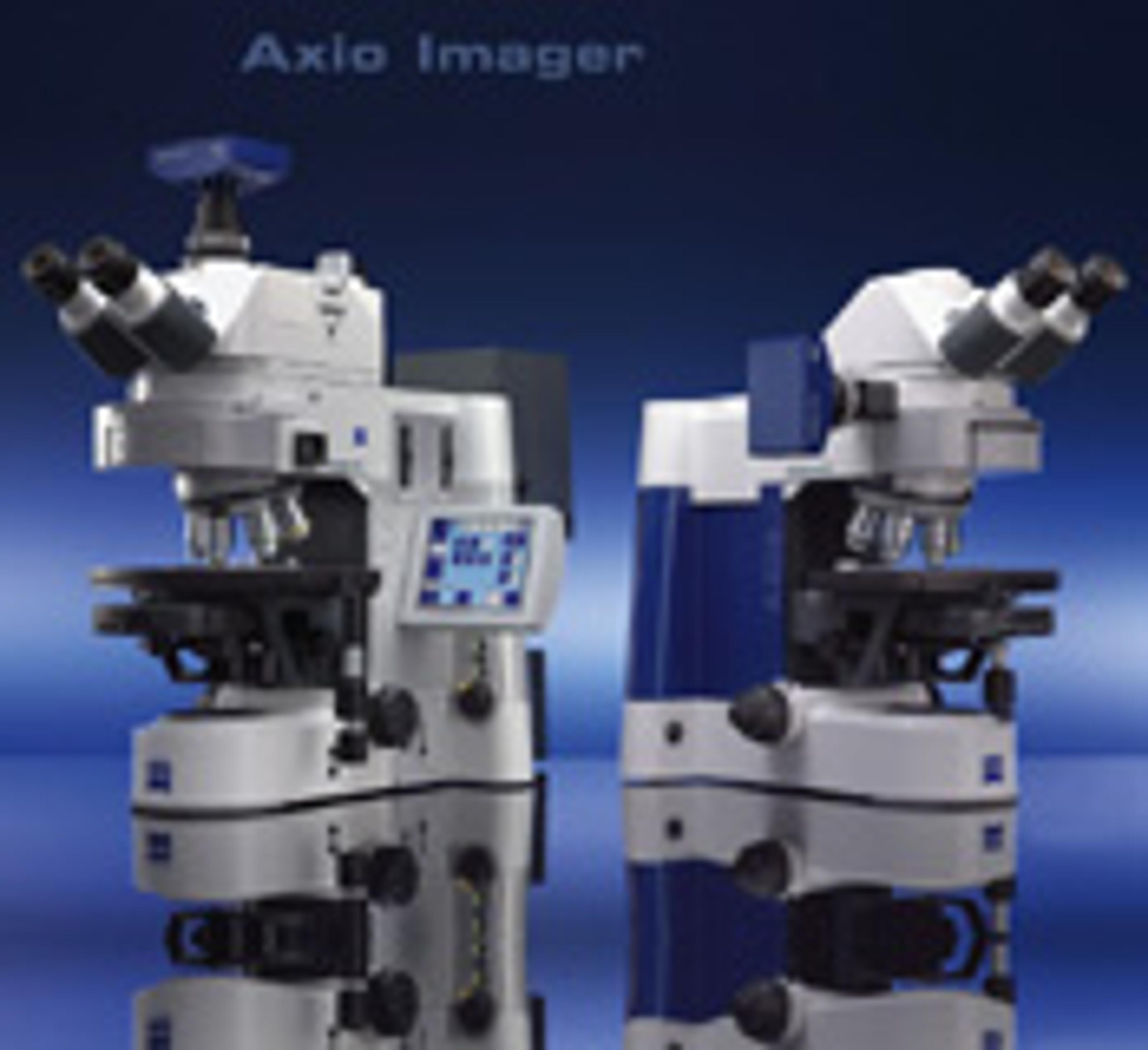
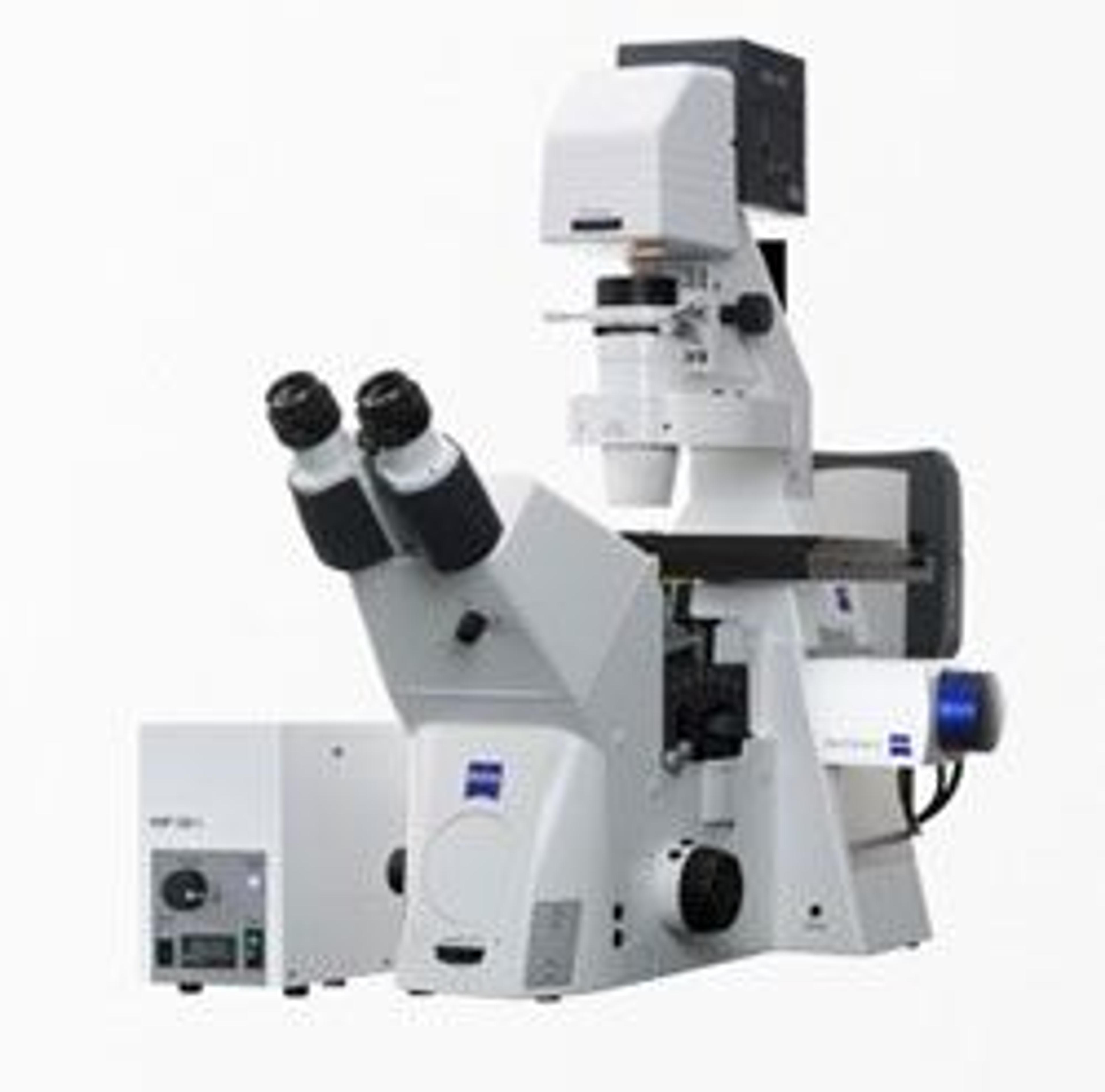
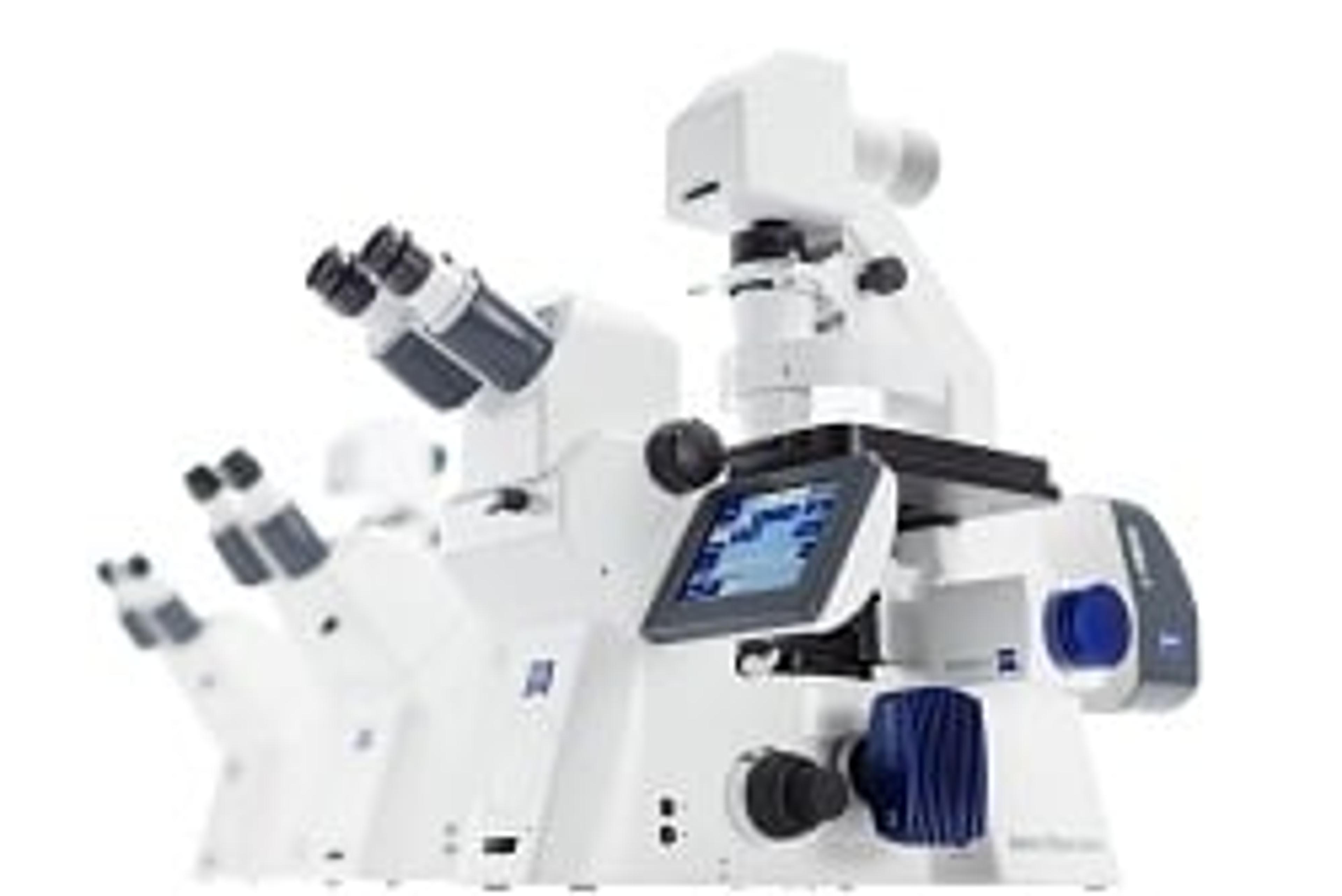
ZEISS GeminiSEM Family
For Your Highest Demands in Sub-nanometer Imaging, Analytics and Sample Flexibility


Receive your quote directly from the manufacturer.
Zeiss microscopes are very good equipment, precise, robust and affordable.
electronic devices and materials
I used Zeiss microscopes and I can testify that they are very good equipment, precise, robust and affordable referring to cost, I recommend Zeiss equipment.
Review Date: 26 May 2023 | ZEISS Research Microscopy Solutions
Very good instrument to learn about new things.
We use FESEM for Imaging, Material analysis, Micro manipulators and thermal analysis
Ease of Use: User friendly software, It is easy to change manipulator system and heating module. After Sales Care is good within the warranty period, after that AMC is required to take care of the instrument. Overall instrument is value for money because of its reliability and performance.
Review Date: 14 Dec 2022 | ZEISS Research Microscopy Solutions
Reliable tools, have accompanied me since I started in research
Semiconductors and Graphene
Robust, precise, and versatile.
Review Date: 8 Jul 2022 | ZEISS Research Microscopy Solutions
Great results
Thin film and compounds
Great results
Review Date: 24 Mar 2022 | ZEISS Research Microscopy Solutions
Great
Nanoscience
This brand provides excellent machines with high quality and have fast after sales service
Review Date: 24 Jan 2022 | ZEISS Research Microscopy Solutions
Highly reliable, world class reproducible results at an affordable price.
Materials science and nanotechnology
We have been using Zeiss SEM system (3 numbers) for several years. It is an indispensable tool for research in materials science and nanotechnology. It has been serving us for decades with world class data and results are very impressive. The performance is very good and results are reproducible. Its highly recommended and good value for money. It is very affordable. highly recommended. for research. We have been producing high quality data using this machine and their after sales service is very good. There are a large number of researchers using this machine for decades.
Review Date: 18 Jun 2021 | ZEISS Research Microscopy Solutions
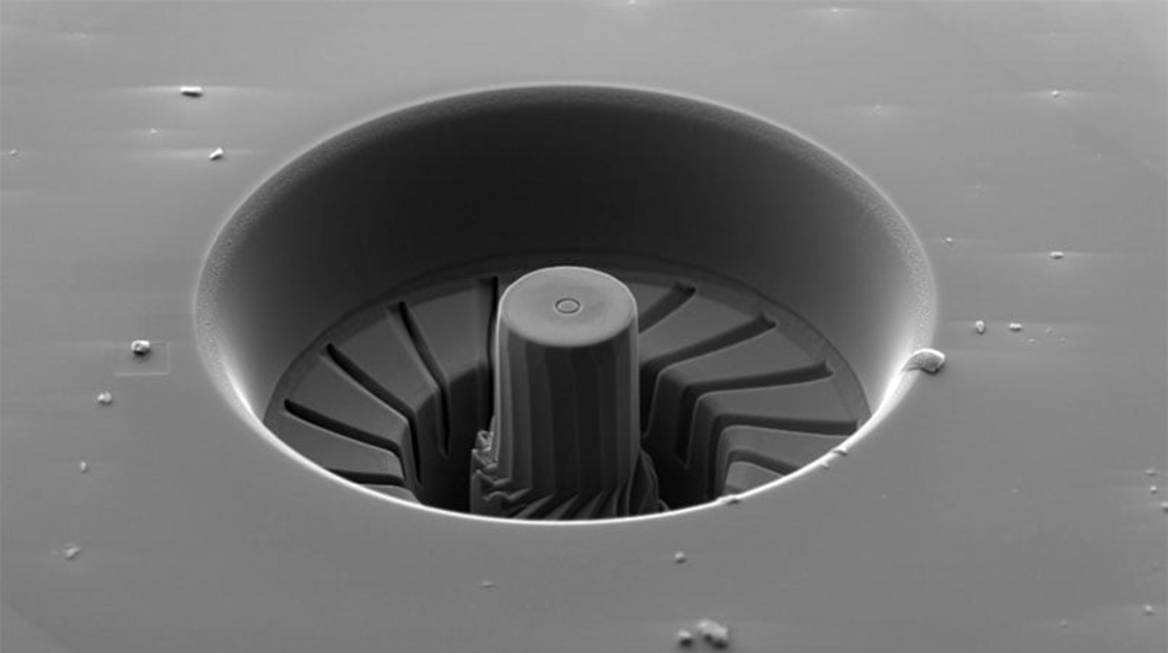
ZEISS GeminiSEM stands for effortless imaging with sub-nanometer resolution. Use it for your most demanding projects in materials and life science. Innovations in electron optics and a new chamber design let you benefit from better image quality, usability and flexibility. Combine excellence in imaging and analytics. Take sub-nanometer images below 1 kV without an immersion lens. Discover three unique designs of the Gemini electron optics. Explore, how ZEISS GeminiSEM family answers all your imaging and analytical needs.
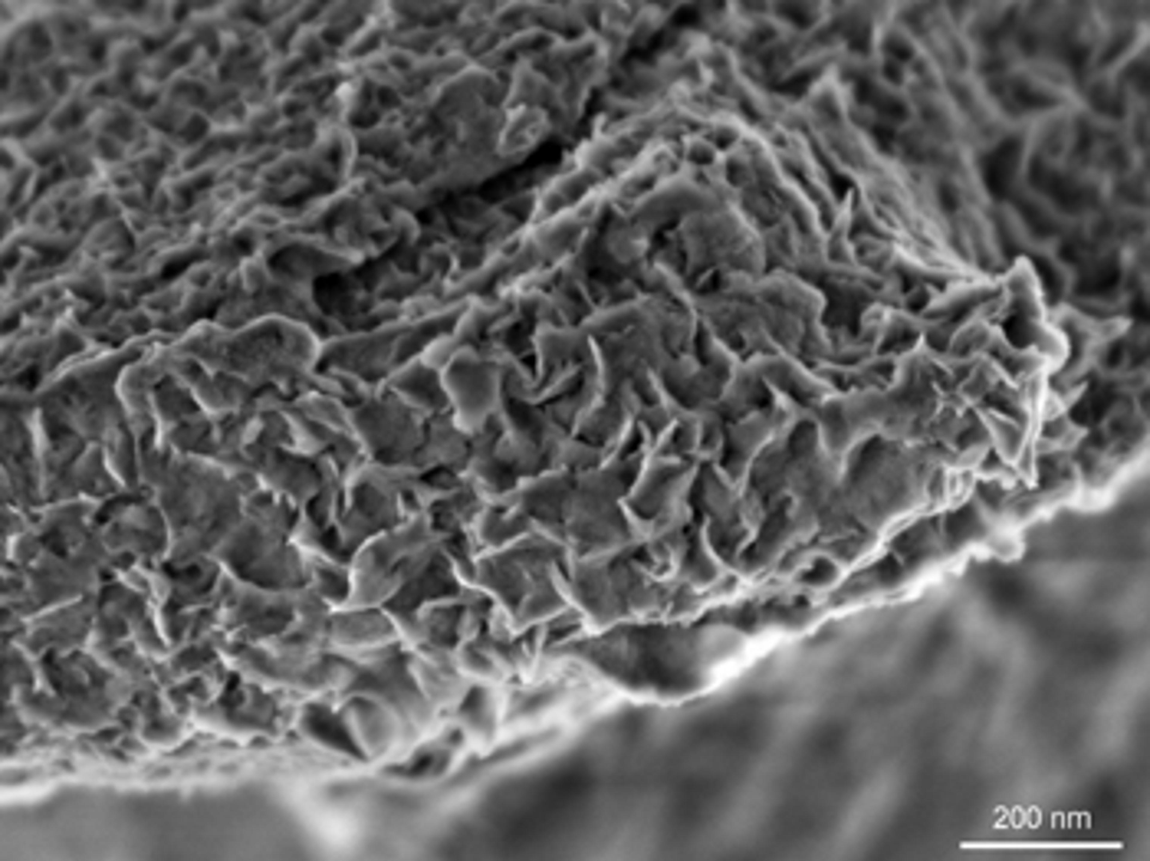
- Characterize nanometer-scaled features at the fractured surface of the non-conducting mineral montmorillonite
- Ideal for core facilities - ZEISS GeminiSEM 360 with its Gemini 1 electron optical column delivers high resolution imaging and analytics over the widest range of applications and sample types
- Enabling efficient analysis - ZEISS GeminiSEM 460 and its Gemini 2 column serve the most challenging tasks in analytical microscopy. Switch seamlessly between imaging and analytical conditions over a wide range of probe currents.
- The new standard for surface imaging – introducing ZEISS GeminiSEM 560, Gemini 3, and its new electron optical engine Smart Autopilot. It delivers the highest resolution in the family at all working conditions.
Brochures

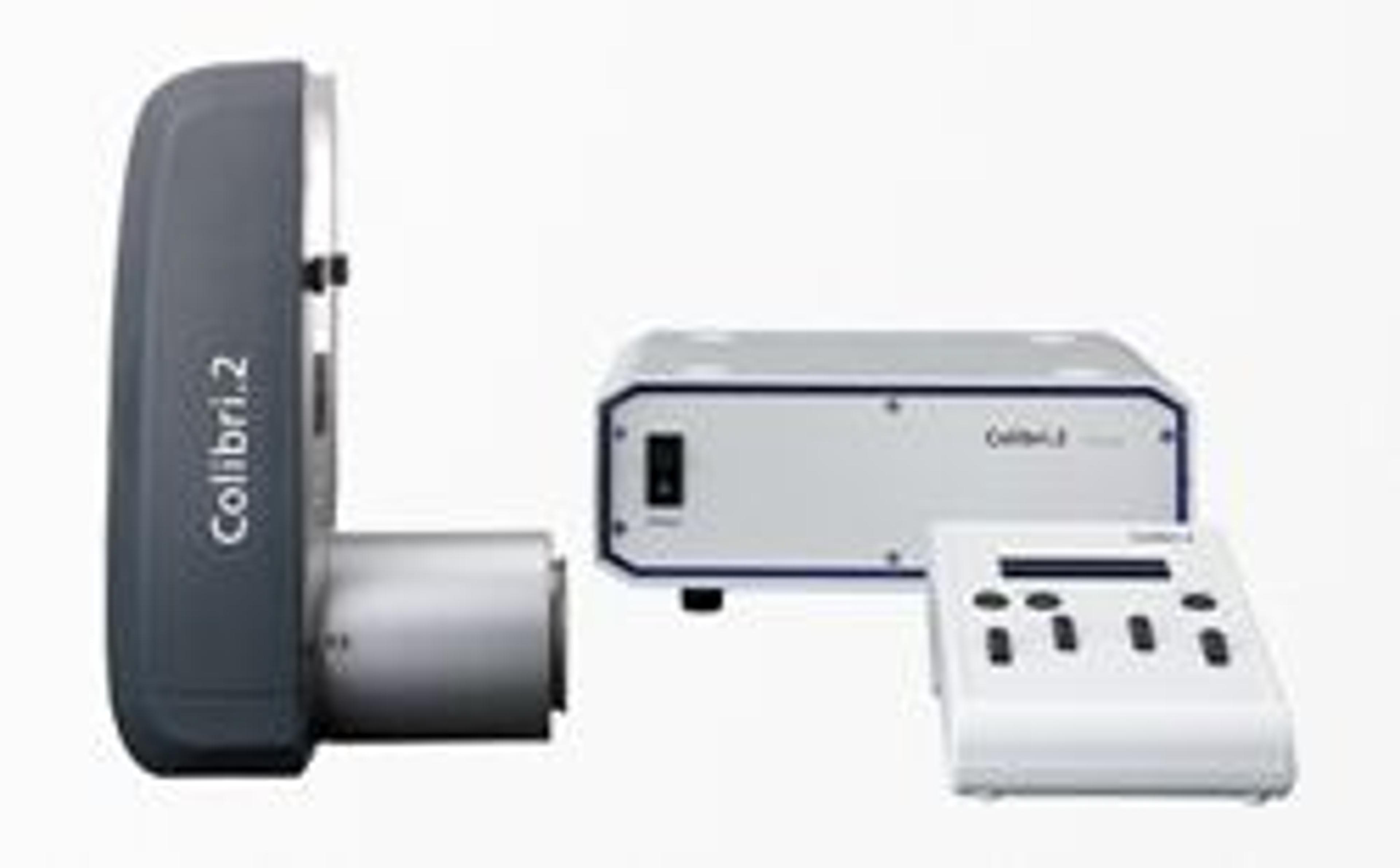
ZEISS integrated atomic force microscope: Your only true in situ AFM solution for FE-SEMs and FIB-SEMs
This product brochure describes the features of the ZEISS integrated atomic force microscope - a combination of atomic force microscopy (AFM) with your ZEISS scanning electron microscope (SEM) or focused ion beam-SEM (FIB-SEM).
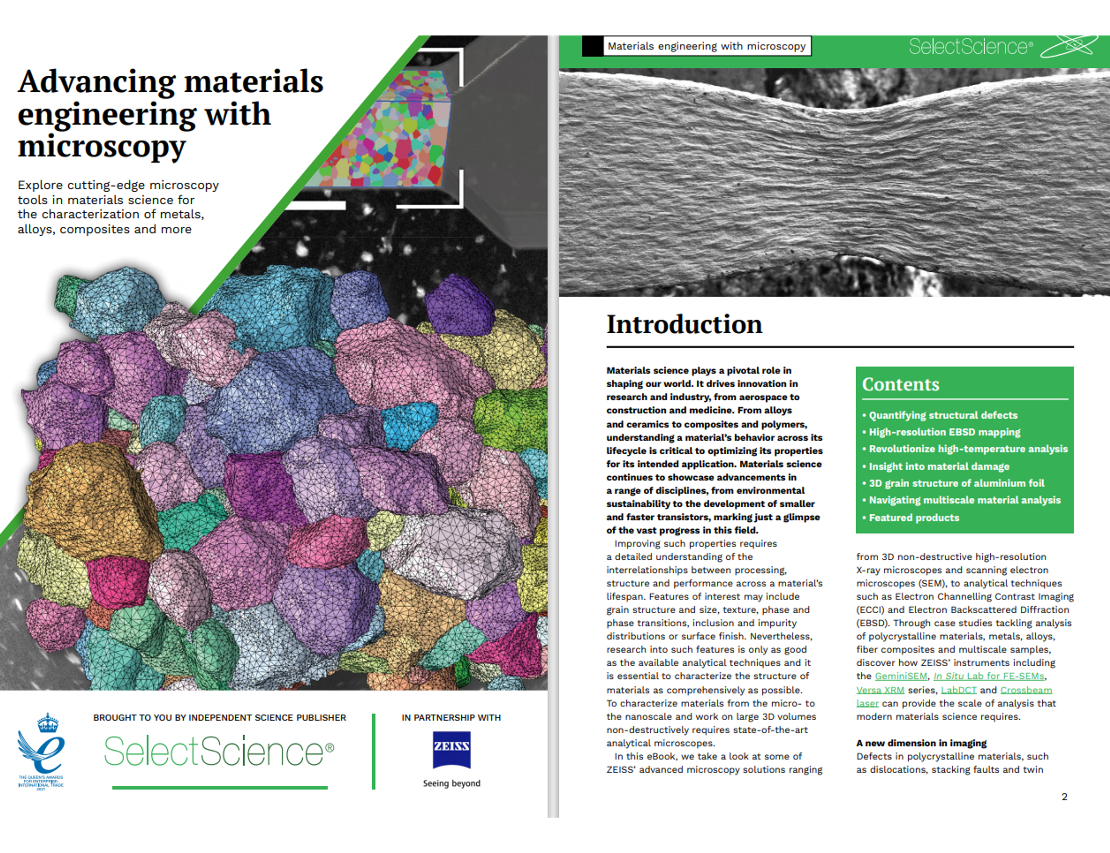
Advancing materials engineering with microscopy
Materials science is crucial in shaping our world and driving innovation across various fields like aerospace, construction, and medicine. It involves understanding the behavior of materials such as alloys, ceramics, composites, and polymers throughout their lifecycle. This knowledge is essential for optimizing their properties for specific applications.
Download this expert guide for free today and explore advanced microscopy solutions from ZEISS, including 3D non-destructive high-resolution X-ray microscopes and scanning electron microscopes (SEM). The eBook also covers analytical techniques such as Electron Channelling Contrast Imaging (ECCI) and Electron Backscattered Diffraction (EBSD).
Plus, find case studies on polycrystalline materials, metals, alloys, fiber composites, and multiscale samples, and learn about the tools essential for modern materials science analysis.
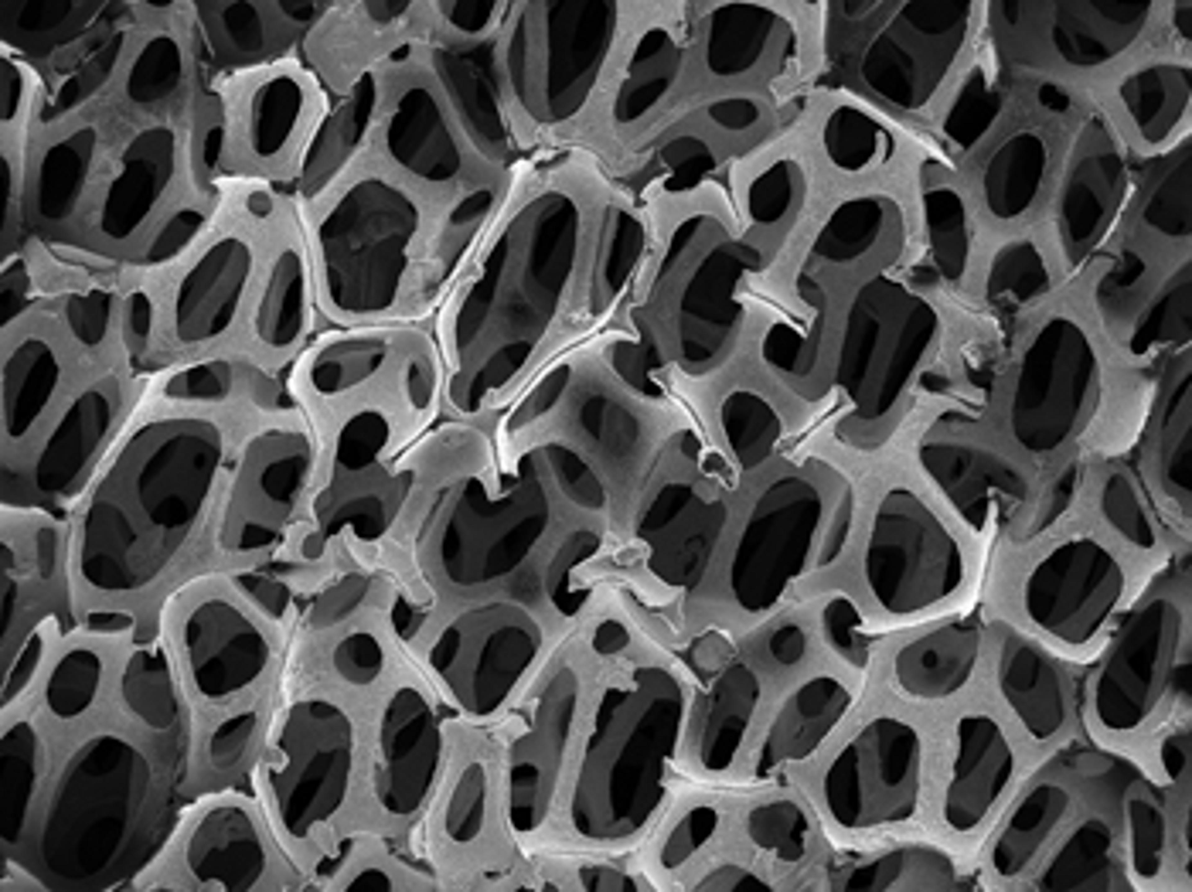
FE-SEM Imaging at 500V
In this application note, Zeiss discusses ultra-low voltage imaging in field emission scanning microscopes. Learn how imaging is performed and how beam damage and charging are avoided. The advantages are illustrated on various materials like polymers, batteries etc.
Evolution of Gemini electron optics: The next chapter in sub-nanometer imaging below 1 kV
In the last 20 years, a major thrust of research in scanning electron microscopy (SEM) has been driving the performance of systems towards higher resolution at lower voltages. Key to the performance of any SEM, conventional or field emission SEM (FE-SEM), is its electron optical column.
In this application note, ZEISS demonstrate the evolution of their FE-SEMs, which are based upon the Gemini column design which has seen a number of technological advancements since it was first launched in 1993. The latest development in this field is the new engine Smart Autopilot which provides further increases in resolution at low kV by optimizing the convergence angle of
electrons travelling through the column at given conditions.
Novel Optical Design of Field Emission SEMs
Field emission scanning electron microscopy is standard technology for high resolution imaging and different contrasting methods aiming for a comprehensive characterization of specimens. A wide range of applications is covered by classical FE-SEM technology, including imaging surface sensitive and non-conductive samples without pre-treatment. This application note demonstrates the utility of Zeiss' Gemini technology in advanced imaging applications.
Improving High-Resolution Imaging of Non-Conductive Specimens with Local Charge Compensation
High-resolution combined with an additional expansion of analytical capabilities is extremely important for many applications in material analysis. With the integration of a charge compensation system, these investigations are not restricted to conductive samples only but can also be executed for all kinds of non-conductive samples. Such a method is demonstrated here in the application note below.
ZEISS Gemini Optics: High-Resolution Images with Real-World Samples
In this poster, ZEISS demonstrates the capacity of Gemini Optics with a variety of real-world samples, ranging from metal particles to biological materials.
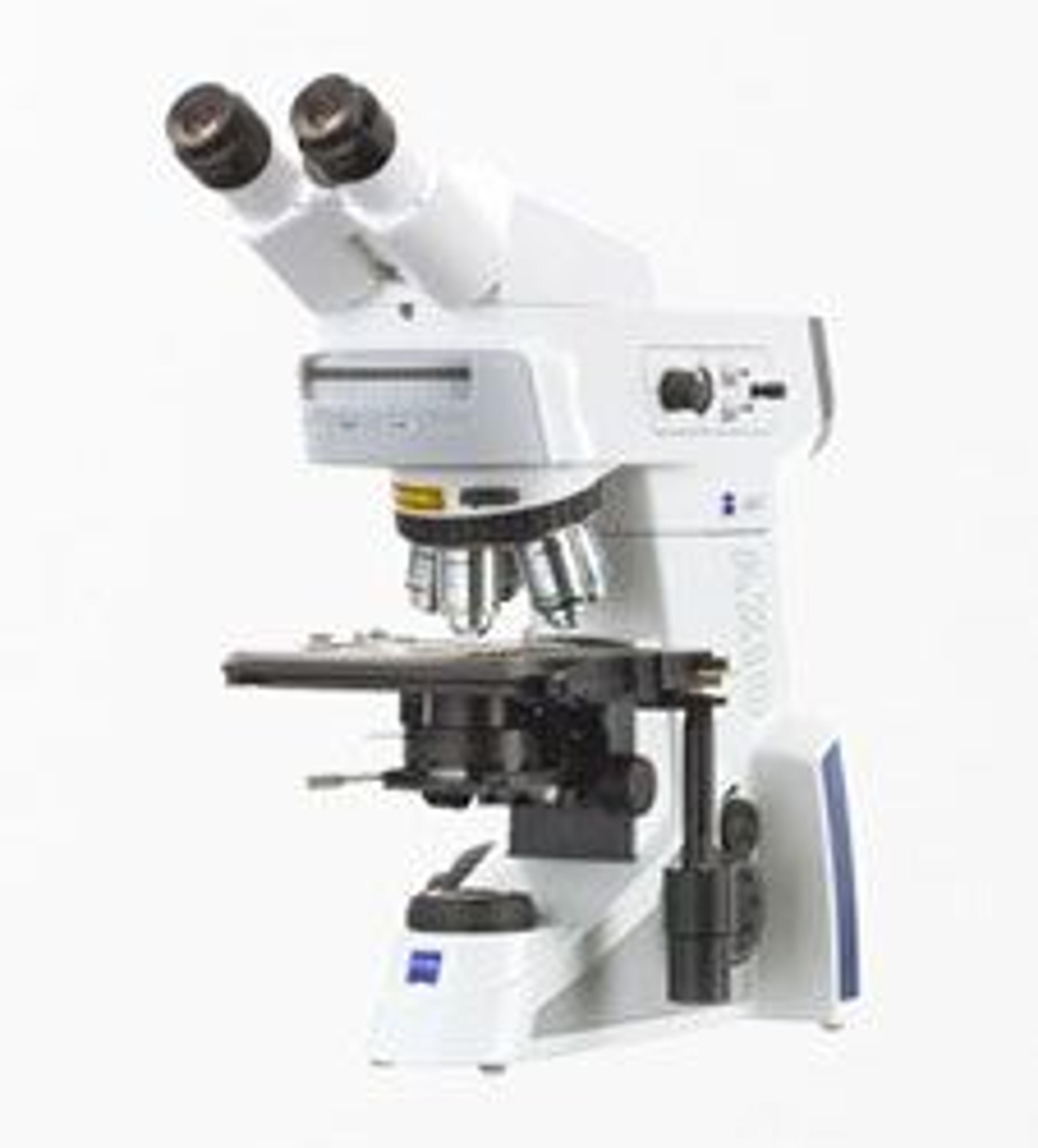
ZEISS Microscopy Solutions for Steel and Other Metals
ZEISS Microscopy offers multi-modal characterizations and advanced analysis options for industry and research. This application note provides a variety of applications of ZEISS products to analyze steel and other metals.
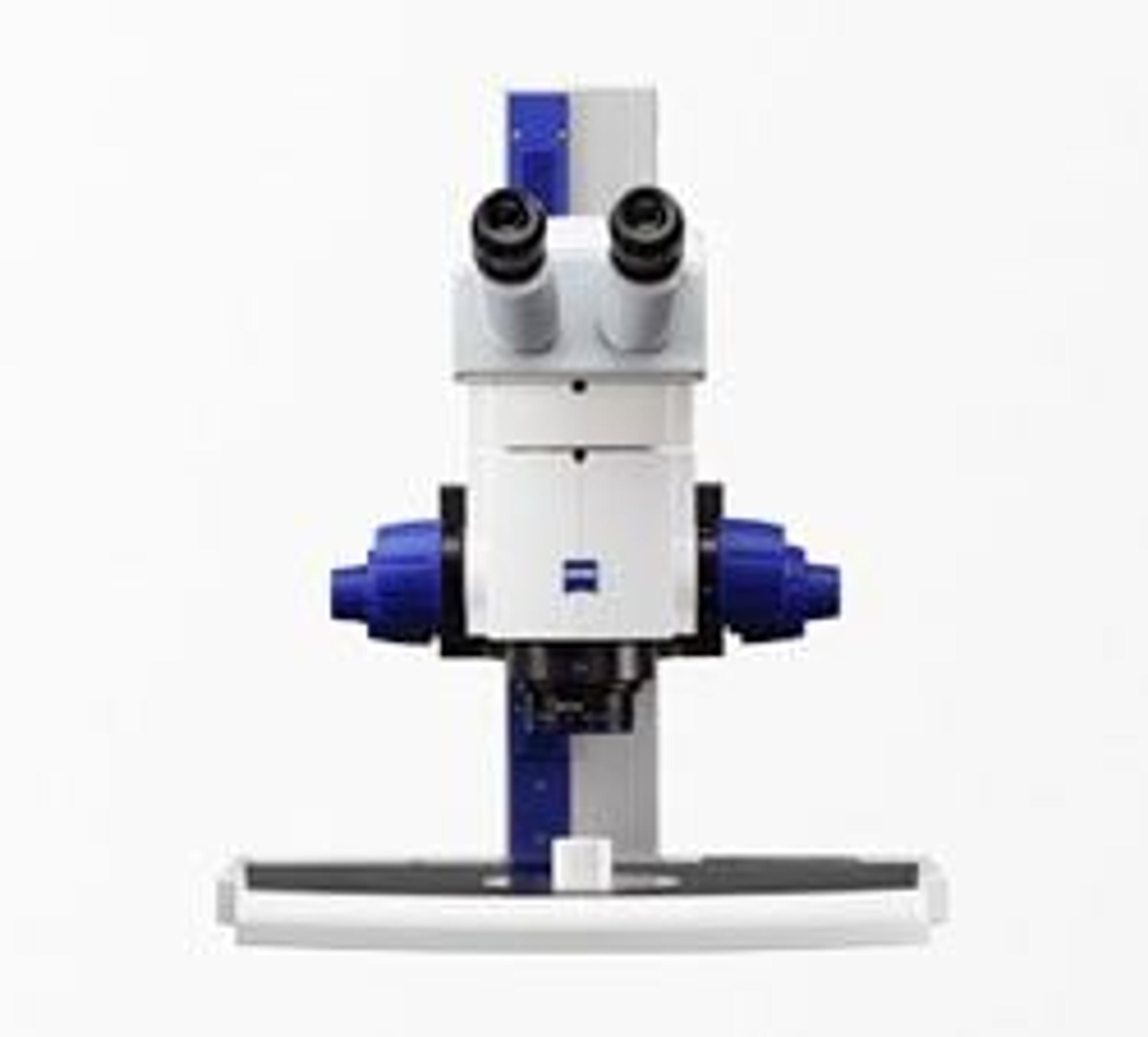
Combining AFM and SEM for High Performance Visualization
ZEISS in situ AFM optics integrates the best qualities of AFM and SEM to deliver high-performance in visualizing 3D topography down to the atomic level while measuring a wide range of physical properties. To find out more about the applications of in situ AFM, check out the appnote below.
How to Choose the Best GeminiSEM Field Emission SEM for Your Research
The GeminiSEM serie stands for effortless imaging with sub-nanometer resolution and high detection efficiency. You can rely on its surface sensitive analysis and profit from the highest sample flexibility. The appnote below provides essential guidances to choose the best GeminiSEM product for your research, industrial lab, imaging facility or educational organization.
Fast Imaging and Analysis with High Probe Current and High Resolution
This application note explores the capabilities of the GEMINI II column found in the ZEISS MERLIN FE SEM, including: short image acquisition times at high resolution for mosaics, 3D data collection and fast mapping for chemical analysis (EDS) and crystallography studies (EBSD) over a wide range of materials and applications.
Battery centric workflows for next-generation battery developments
Tuesday, July 28 at 16:00 BST | 17:00 CEST | 11:00 EDT | 08:00 PDT
Want to know how to design battery-centric workflows, handle air-sensitive samples, and connect glovebox, FE-SEM, and XRM?
The development of high-energy-density chemistries, recycling methodologies, and the optimization of lithium-ion systems rely on characterization methods to provide a feedback loop between microstructure, processing, and electrochemical behavior.
In this SelectScience® webinar, we will examine how today’s microscopy workflows address battery research, including Li- and Na-based solid-state batteries. You will learn how to design 'battery-centric' workflows that connect destructive and non-destructive methods to specific research questions, including:
- What is the microstructure of an electrode, including its 3D nanoscale architecture, and how is that linked to electrochemical performance?
- How are components and microstructures arranged and aligned inside an assembled battery, and how do they evolve during cycling?
- How can battery and electrode microstructures be assessed coherently across different length scales?
- How can battery recycling be optimized from the efficient characterization of black mass powder in multiple dimensions?
The first part of this webinar will focus on handling air-sensitive materials using air-free transfer workflows that bridge glovebox environments with multiple electron microscopy modalities, enabling investigation of microstructure, while preserving the native state as much as possible.
The second part will highlight X-ray microscopes (XRM) as a non-destructive, minimal-preparation technique for 3D multiscale characterization of intact cells and complex samples such as black mass from recycling processes.
The overall focus will be on research-driven case studies and practical workflow strategies, illustrating how combined destructive and non-destructive microscopy approaches can provide deeper insight into battery behavior, degradation, and lifetime for the battery circular economy.
Certificate of attendance
If you attend the live webinar, you will automatically receive a certificate of attendance, including a learning outcomes summary, for continuing education purposes. If you view the on-demand webinar, you can request a certificate of attendance by emailing editor@selectscience.net.
Webinar details
- Cost: Free to attend
- Location: Online
- Duration: 60 minutes
Registration is required to secure your place. If you register but can’t attend live, you will receive a link to the on‑demand recording once it becomes available.

Microscopy with ZEN core: A unified approach to imaging and analysis
April 29, 2025 - 09:00 BST / 10:00 CEST / 16:00 CST / 17:00 JST
Join us for an informative webinar sponsored by ZEISS, where we will introduce ZEN core, a sophisticated software solution designed to enhance your microscopy workflows. This session will focus on how ZEN core provides a streamlined user interface that accommodates both light and electron microscopy, allowing users to transition seamlessly between modalities.
During the session, you will discover how ZEN core's intuitive user interface adapts to the unique needs of your laboratory allowing users of all experience levels to efficiently image, analyze, and manage data. We will explore the advanced imaging capabilities, automated workflows, and powerful AI features that make ZEN core the command center for both light and electron microscopes.
Join us for a live demonstration of ZEN core and take part in our Q&A session to address your specific inquiries. Register today to learn how ZEN core can support your microscopy research and analysis needs.
Key learning objectives:
- Understand how ZEN core fosters seamless collaboration in connected laboratory environments
- Explore the integration of multiple microscopy techniques within a unified platform
- Learn how ZEN core ensures data consistency and standardization across instruments and locations
Who should attend?
This webinar is ideal for researchers in both academia and industry looking to improve their microscopy practices and enhance productivity.
Certificate of attendance
All webinar participants can request a certificate of attendance, including a learning outcomes summary, for continuing education purposes.
If you view the on-demand webinar, you can request a certificate of attendance by emailing editor@selectscience.net.
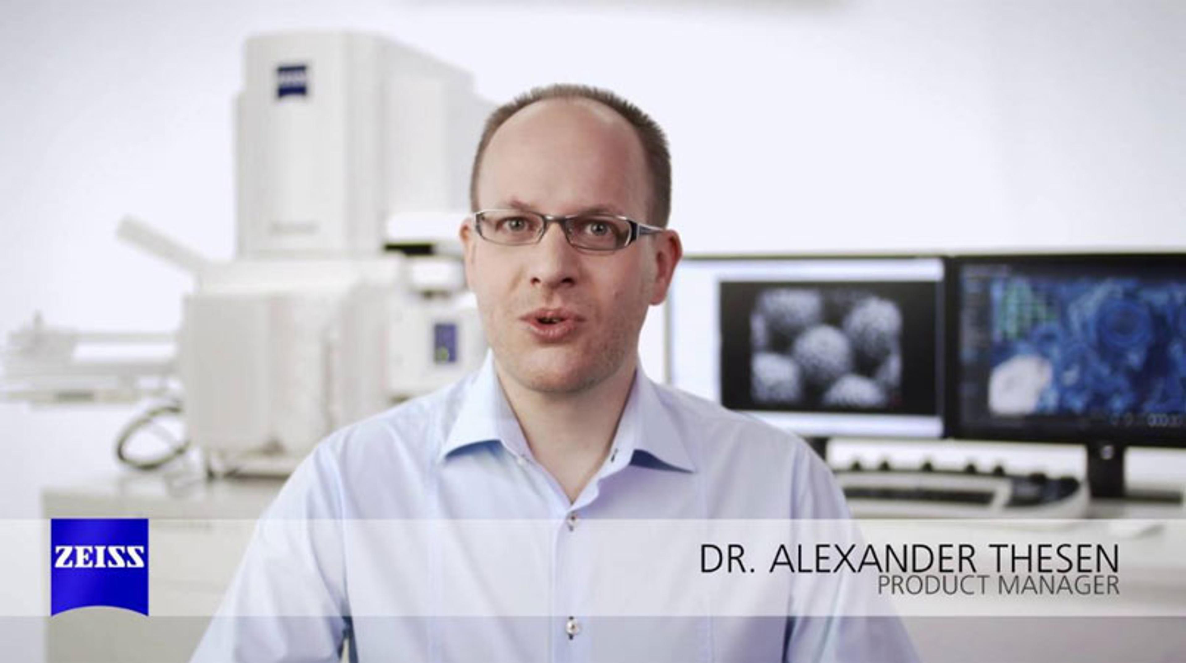
Advanced Imaging With the ZEISS GeminiSEM Family
In this introductory video, Dr. Alexander Thesen, product manager at ZEISS, describes the advantages of the ZEISS GeminiSEM Family.
How ZEISS Microscopes are Shaping the Future
In this video, learn how ZEISS is developing technologies for use at the cutting edge of science, consumer electronics, energy, construction, and more.
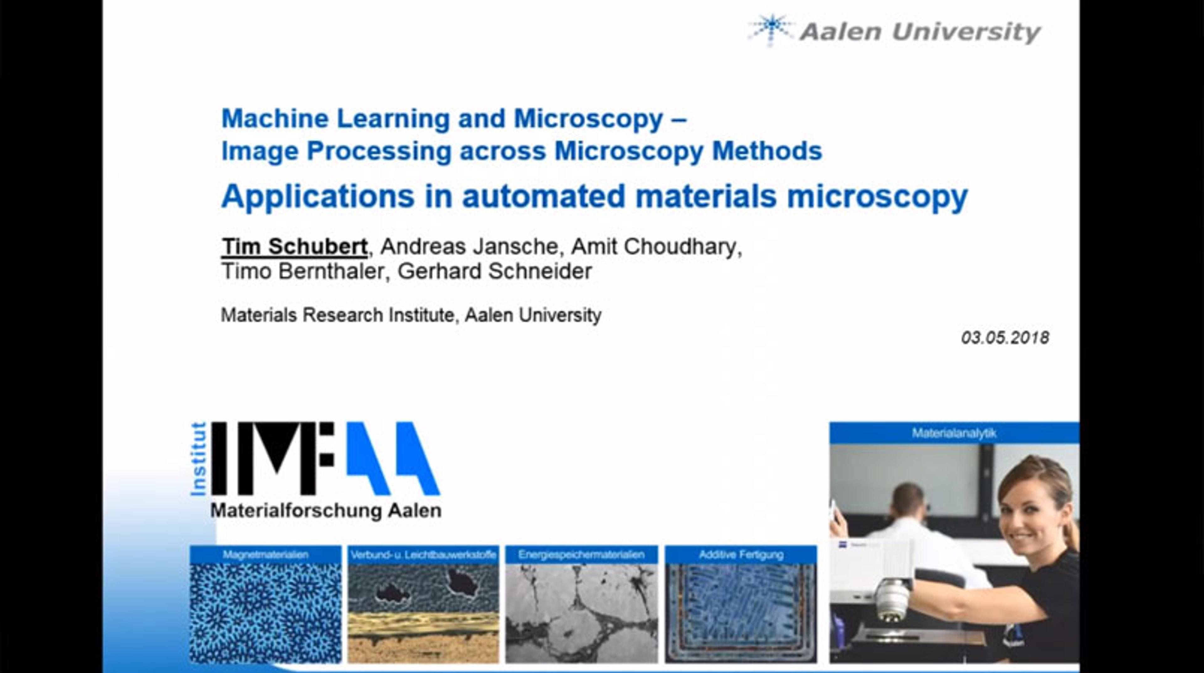
Webinar: How Machine Learning Software Can Accelerate Microscopy Image Analysis
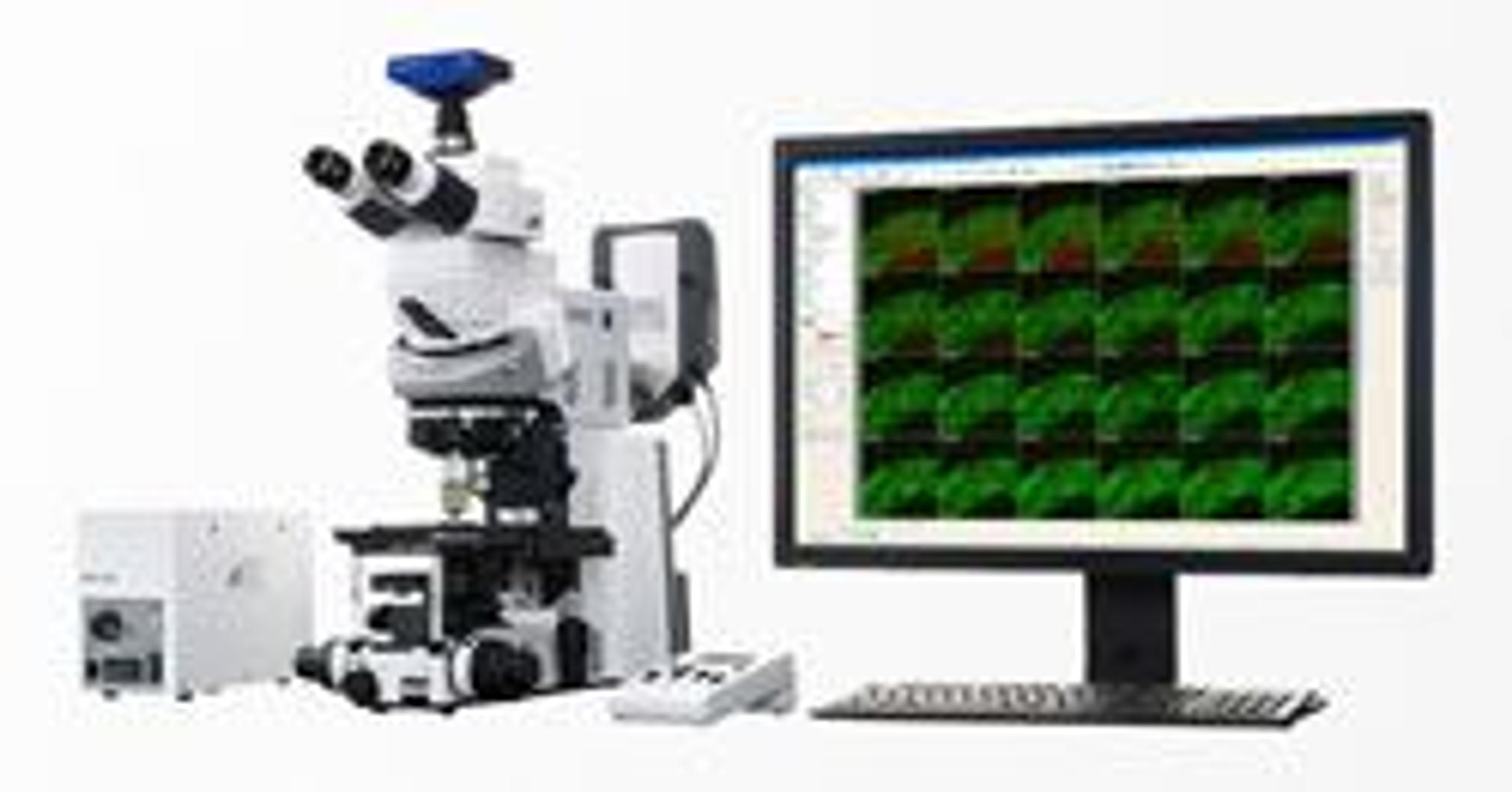
In this webinar, find out how machine learning software, ZEISS ZEN Intellesis, can be applied to speed up and advance image processing capabilities across multiple microscopy methods. Tim Schubert (University Aalen) and Tobias Volkenandt (ZEISS Microscopy) present their latest application examples concerning image analysis and segmentation using machine learning techniques, revealing its excellent application for materials analysis via SEM, FIB-SEM, light microscopy and X-ray microscopy.
WITec ZEISS Partnership Enables Integrated SEM/Raman Workflow
ZEISS Microscopy is partnering with WITec to enhance their advanced scanning electron microscope (SEM) with the addition of Raman technology. In this video, discover how this partnership has enabled the combination of high resolution techniques to create an integrated system which can be used with ease.
From Microscale to Macroscale: ZEISS Microscopy Used to Apply Microscale to Engineering
In this video, Dr. Richard Johnston explains how he uses ZEISS microscopy to investigate the internal structures of both human-made and natural products. The use of non-destructive testing within his research enables the interrogation of microstructures and loading of materials, with the aim of applying the microstructure form and function to engineering and design. Johnston explains how advances and collaborations with ZEISS microscopy are enabling correlative imaging studies.

Latest Gemini technology for ultimate microscopic characterization of challenging samples
Watch this on-demand webinar to find out how the Gemini technology from ZEISS addresses challenging microscopy samples

Secondary ion mass spectroscopy workshop: Sensitive compositional analysis at the micro- and nanoscale
Watch this webinar to gain insight into SIMS technology and discover an innovative solution offering the world record in SIMS lateral resolution
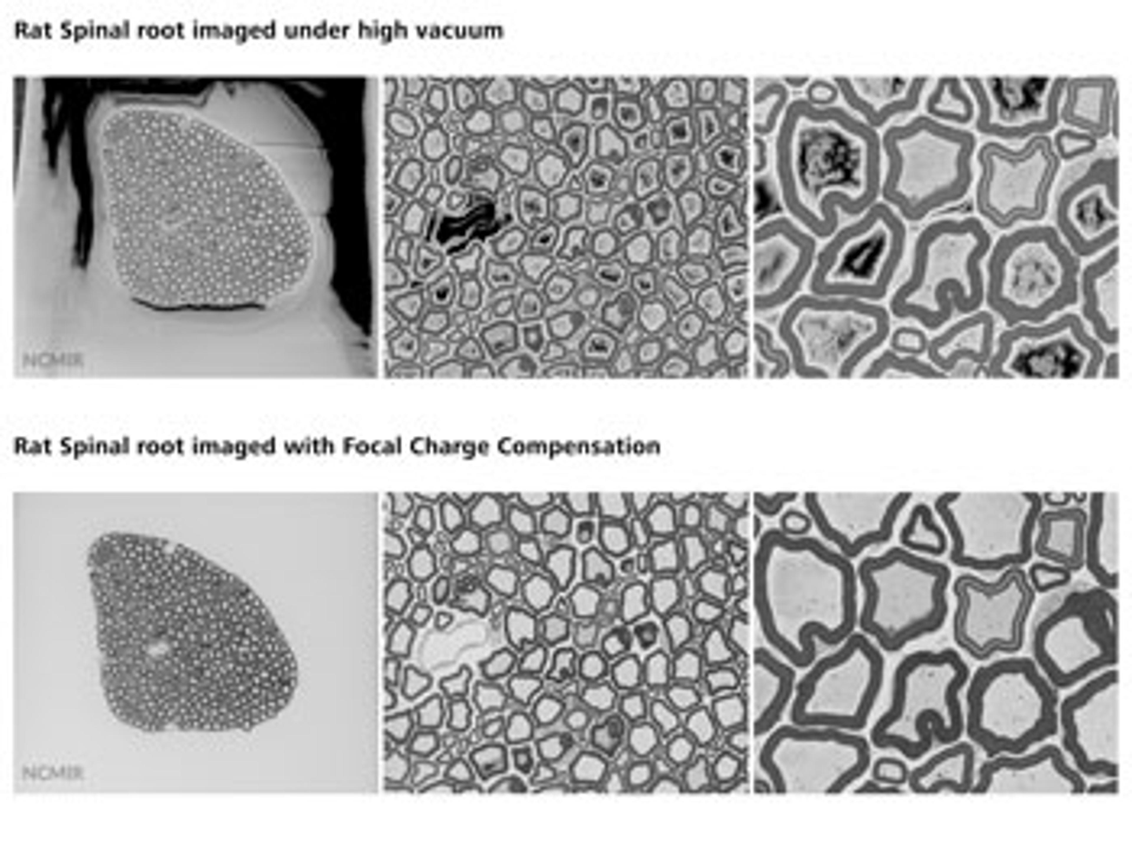
New Focal Charge Compensation Mode for ZEISS Field Emission Scanning Electron Microscopes Improves Image Quality
High-resolution 3D block face imaging for biological samples with fast acquisition rates and minimal sample damage
MATERIALS UPDATE: Pushing Battery and Solar Cell Research to the Next Level…
From news to application articles, discover the latest advances and methodologies in materials and energy research
New Focal Charge Compensation Mode for ZEISS Field Emission Scanning Electron Microscopes Improves Image Quality
High-resolution 3D block face imaging for biological samples with fast acquisition rates and minimal sample damage
ZEISS Opens New Microscopy Customer Center
ZEISS Presents a Wide Range of Microscopes at PITTCON 2017
Visit Booth #1852 to see ZEISS Microscopy products for use in life science research and material analysis
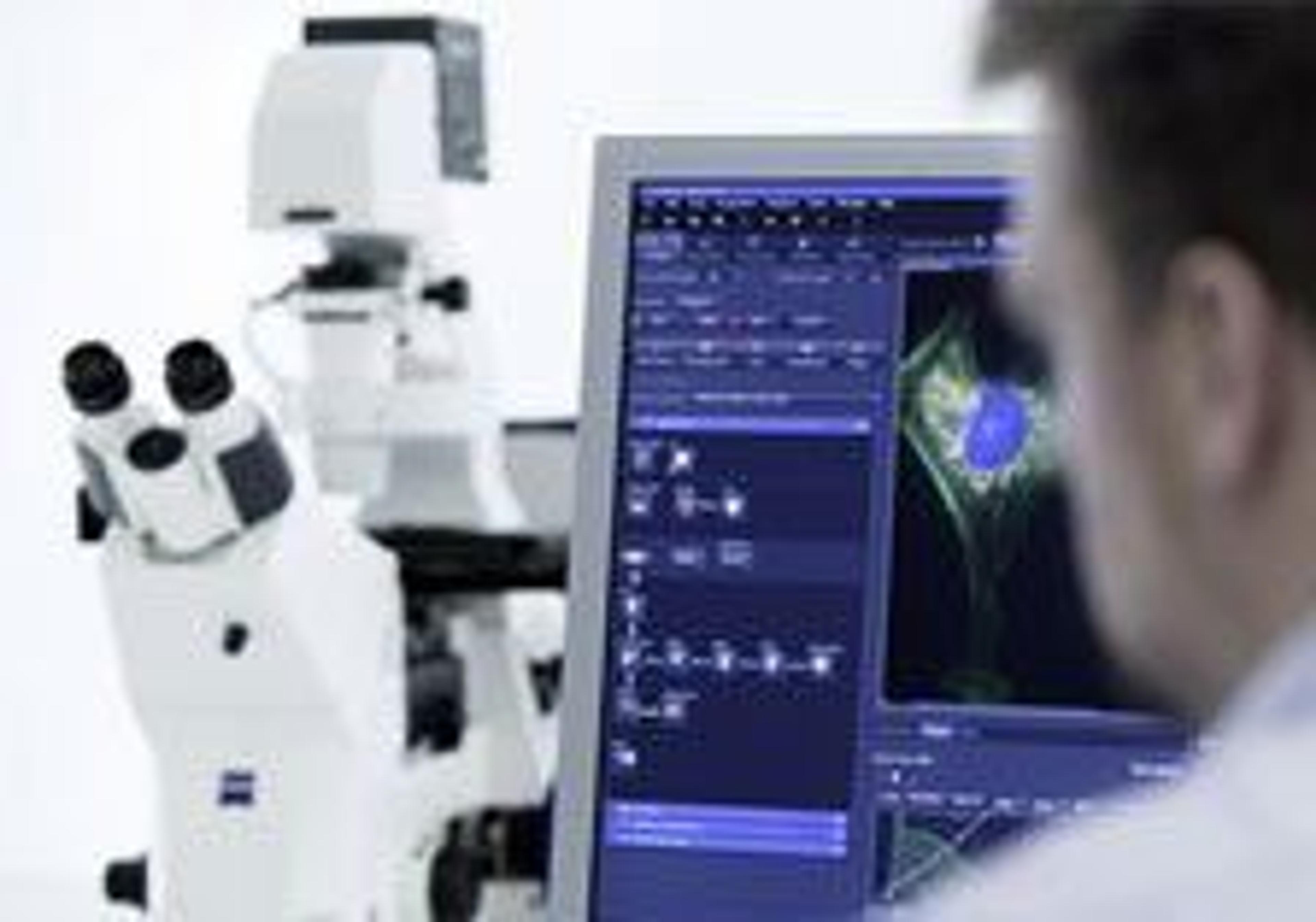
Using Molecular Spies to Understand Changes in Cell State in Health and Disease
SelectScience® spoke to Thomas Deerinck, National Center for Microscopy and Imaging Research at University of California, San Diego, about how correlative microscopy is helping scientists understand disease states