Search
25

Application Note
Viral titer determination


Industry News
Researchers uncover a new CRISPR-like system in animals that can edit the human genome
The first RNA-guided DNA-cutting enzyme found in eukaryotes, Fanzor could one day be harnessed to edit DNA more precisely than CRISPR/Cas systems

Industry News
Key gene that blocks the ‘spillover’ of avian flu to humans discovered
Discovery means targeted solutions can be directed to avian flu viruses sooner to prevent spillover into humans, say scientists
Application Note
Circulating biomarkers application notes


Product Demonstrations
Celloger Mini Plus application: Mitochondrial potential monitoring

Product Demonstrations
Celloger Mini Plus application: Phagocytosis monitoring

Product Demonstrations
Celloger Mini Plus application: Spheroid screening
Product Demonstrations
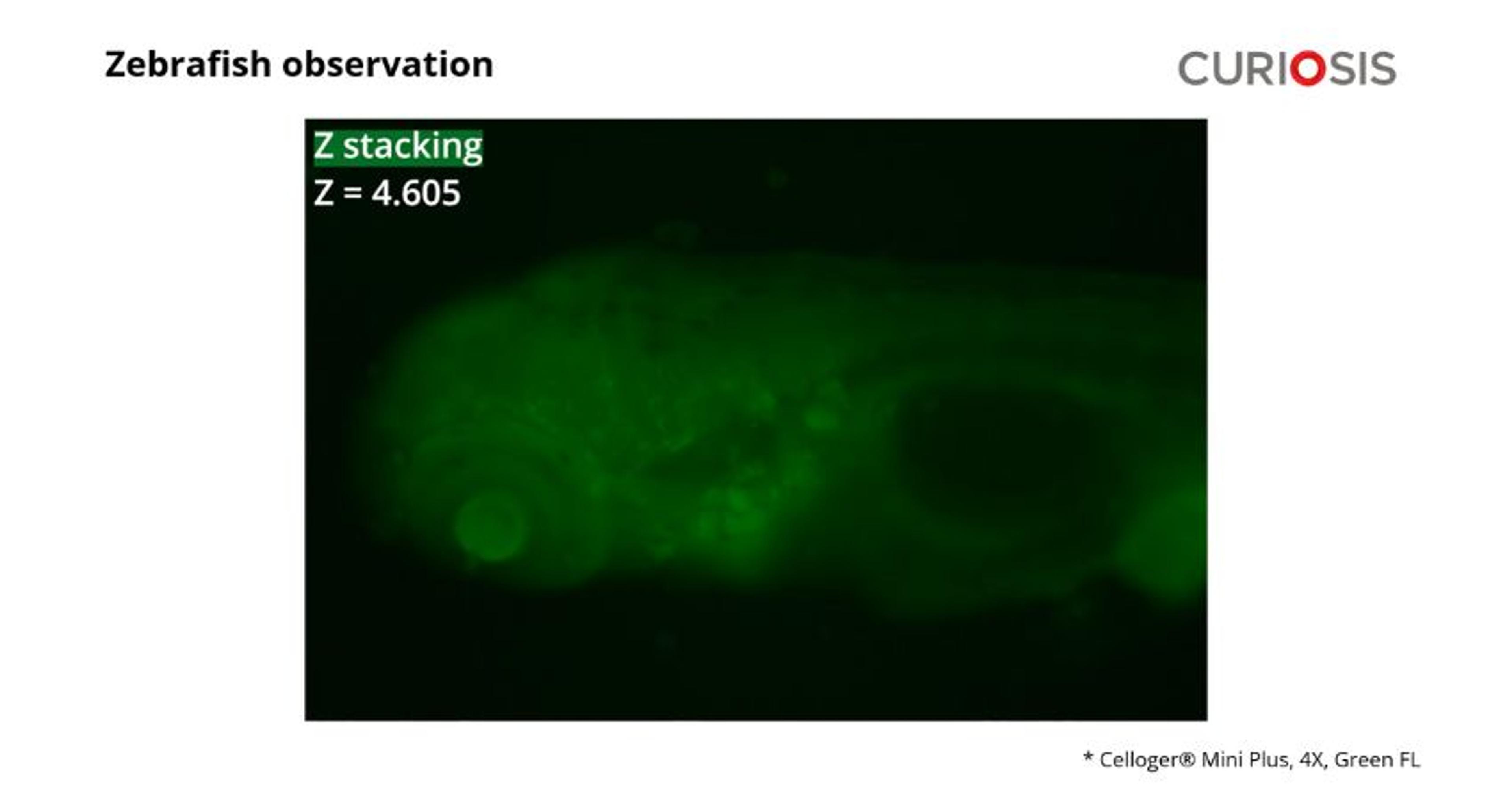
Celloger Mini Plus application: Zebrafish observation
Product Demonstrations
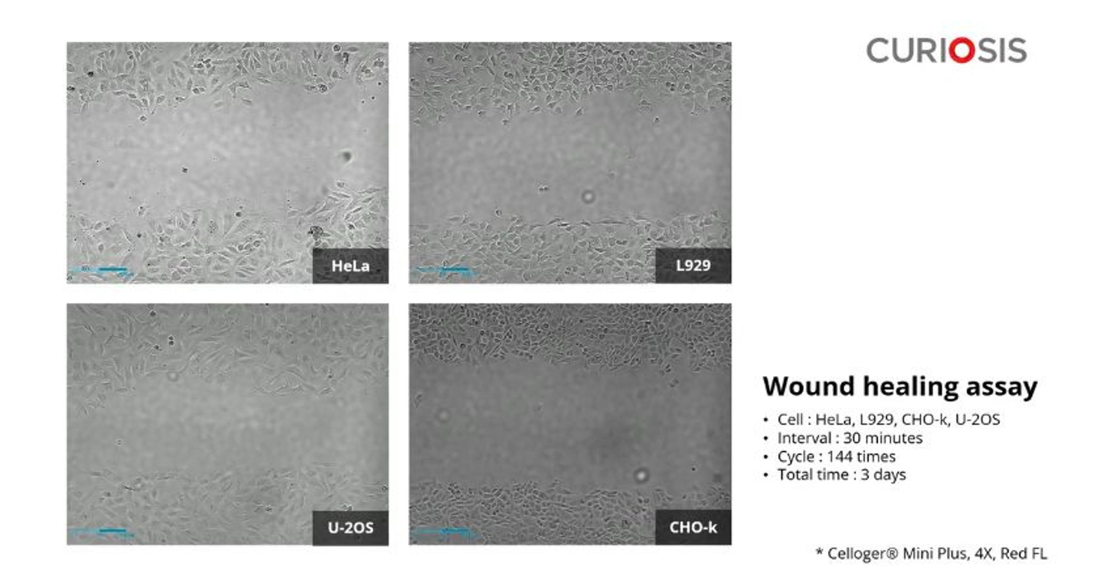
Celloger Mini Plus application: Wound healing assay
Product Demonstrations