
ResourceLife Sciences
High Resolution Imaging of Non-Conductive Specimen Benefits From Local Charge Compensation
7 Jan 2018In this application note, high-resolution SEM imaging is executed on non-conductive samples by the integration of a charge compensation system.
Related products
Request Quote for All Products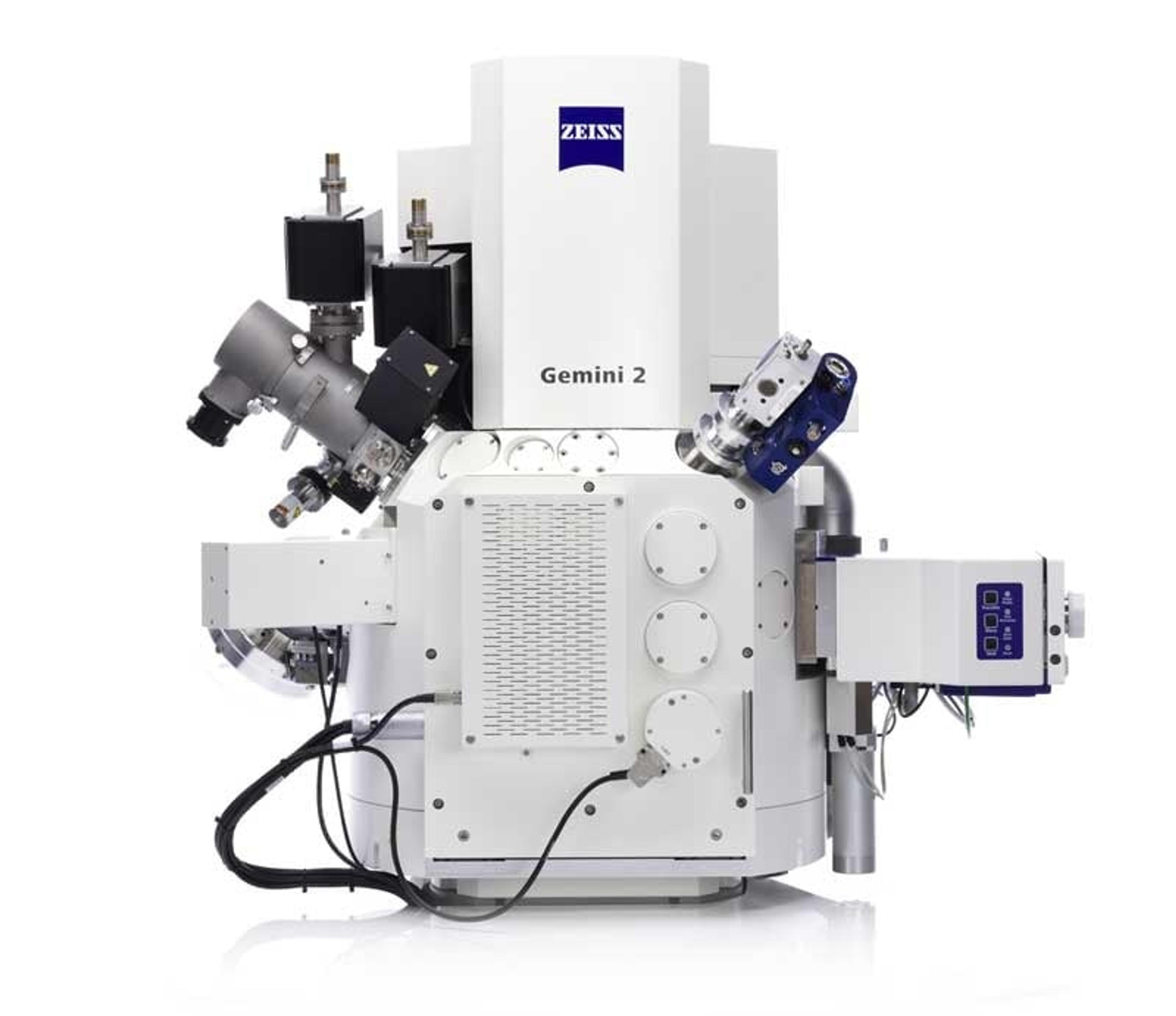
ZEISS Crossbeam Family
ZEISS Research Microscopy SolutionsWithin ZEISS Crossbeam Family you have the choice between Crossbeam 340 or Crossbeam 550. Exploit the variable pressure capabilities of Crossbeam 340. Or use Crossbeam 550 for your most demanding characterizations and choose the chamber size, standard or large, that best suits your samples.
ZEISS GeminiSEM for Life Sciences
ZEISS Research Microscopy SolutionsFor the Highest Demands in Imaging and Analytics from Any Sample
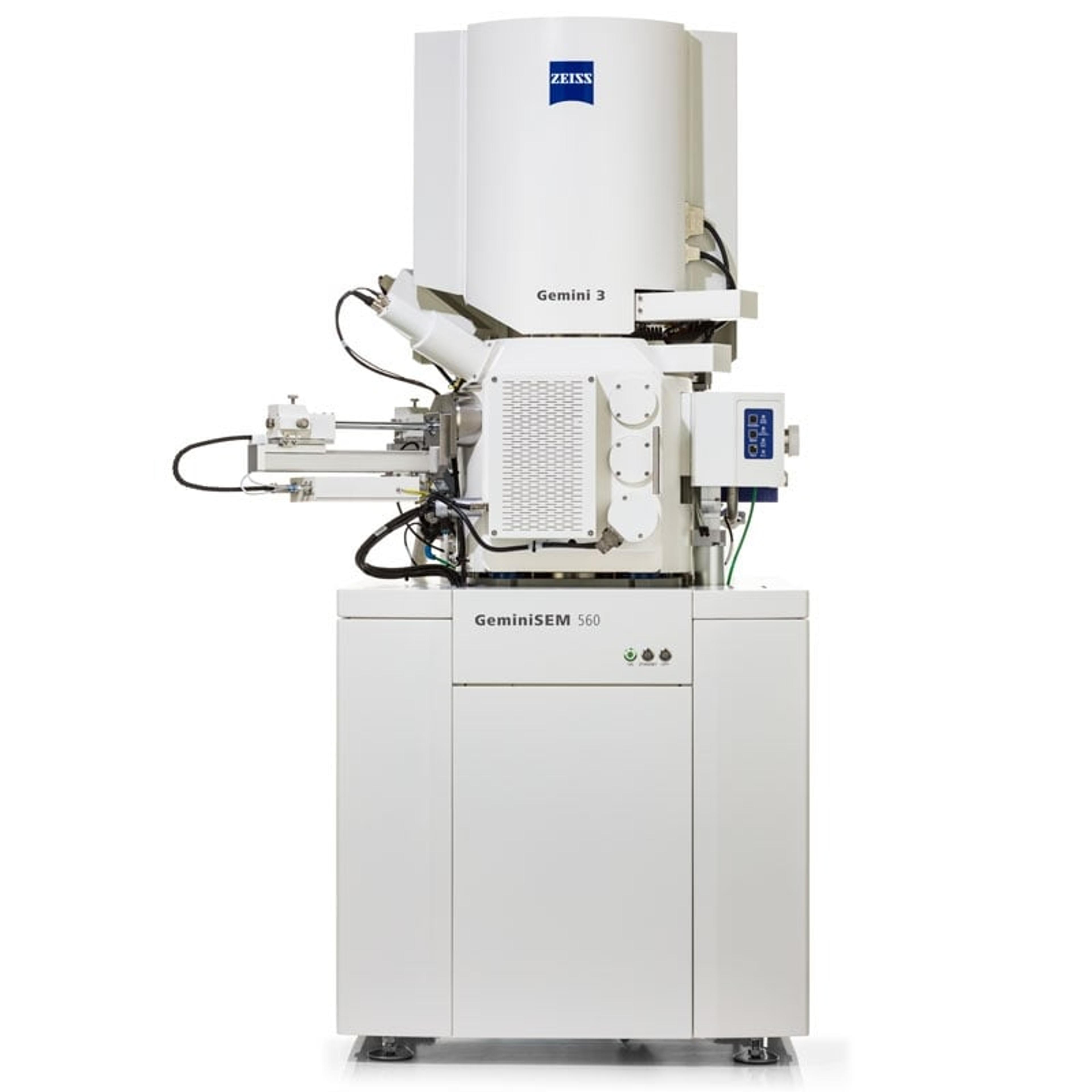
ZEISS GeminiSEM Family
ZEISS Research Microscopy SolutionsFor Your Highest Demands in Sub-nanometer Imaging, Analytics and Sample Flexibility
Links
Tags
Electron MicroscopyElectron microscopes (EM) are used to create high-resolution images of samples at the nanoscale by means of an accelerated beam of electrons as a source of illumination. Types of electron microscope include scanning electron microscopes (SEM), transmission electron microscopes (TEM), scanning transmission electron microscopes (STEM) and cryo-electron microscopes. Focused ion beam (FIB) microscopes are useful for modifying or milling a sample surface with nanometer precision, as well as imaging. Find the best electron microscopes in our peer-reviewed product directory: compare products, check customer reviews and receive pricing direct from manufacturers.