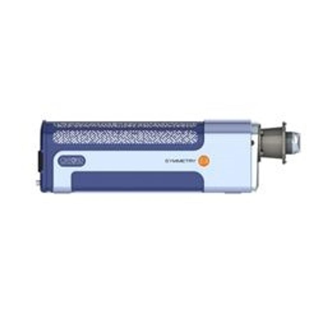
Symmetry® S3
The Symmetry S3 is the only genuine all-in-one EBSD detector on the market, and is based on the revolutionary Symmetry detector, the world’s first EBSD detector to utilise advanced CMOS technology.

Receive your quote directly from the manufacturer.
The Symmetry S3 EBSD detector provides a unique and powerful combination of speed, sensitivity, and diffraction pattern detail through advanced CMOS technology and fibre optics. Symmetry S3, the only genuine all-in-one EBSD detector on the market, has exceptional performance coupled with ease of use, making it the ideal detector for all EBSD applications:
Features:
- Guaranteed indexing speeds in excess of 5700 pps at 156 x 128 pixel EBSD pattern resolution
- 1244 x 1024 pixel resolution – ideal for high angular resolution (HR) EBSD
- Unique fibre-optic coupling with sub-pixel distortion
- Extreme sensitivity, benefiting all types of analysis
- Software controlled detector tilting

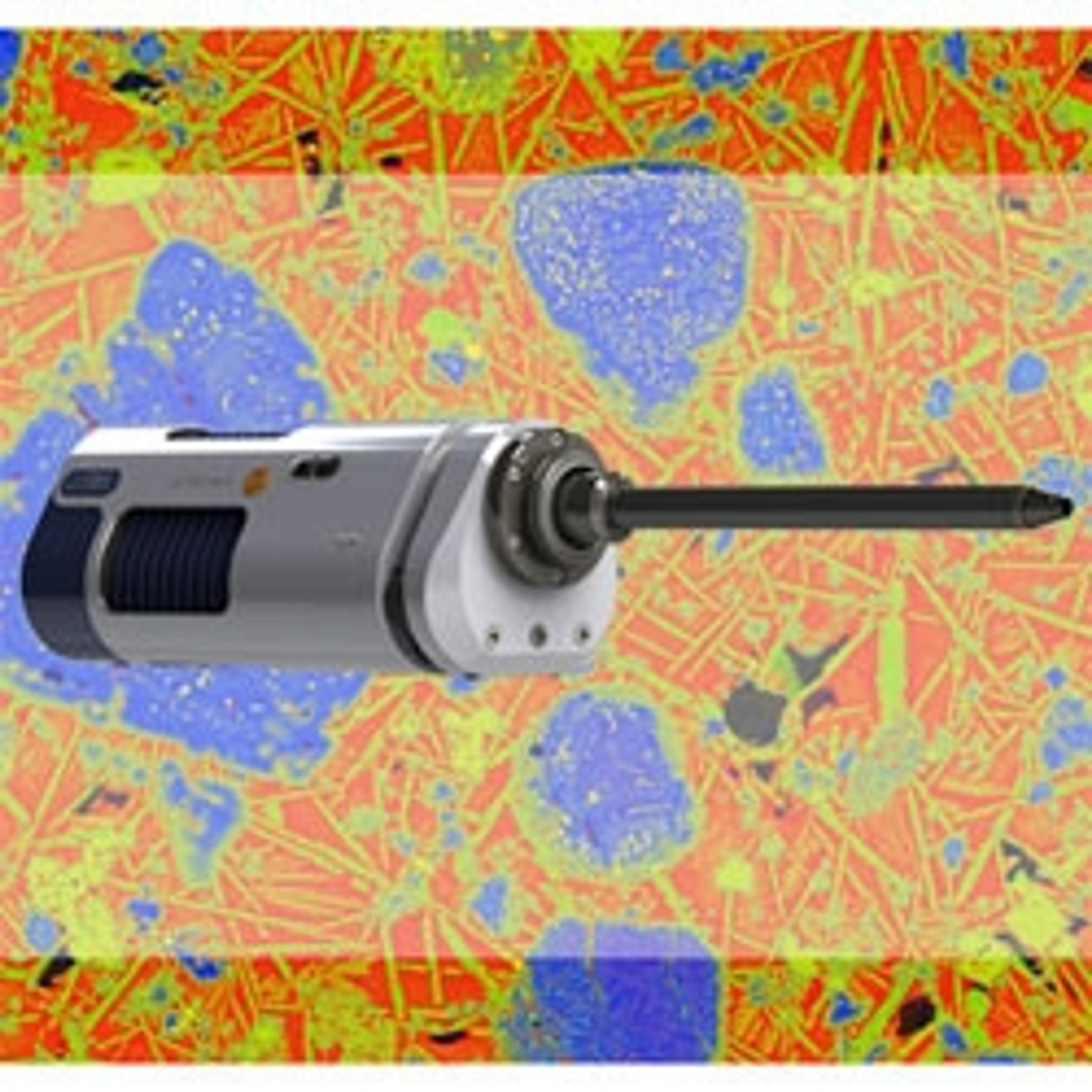
Detailed EBSD study of a bivalve shell
In this application note, Oxford Instruments NanoAnalysis demonstrates how the Symmetry® detector, utilizing custom-developed CMOS technology, is designed to combine sensitivity and speed, making it an ideal detector for analyzing challenging, beam-sensitive, and fine-grained structures such as aragonite nacre. Here, Oxford Instruments NanoAnalysis shows results from routine analyses of calcite-aragonite interfaces in the shell of the mollusk Mytilus edulis (the common mussel).
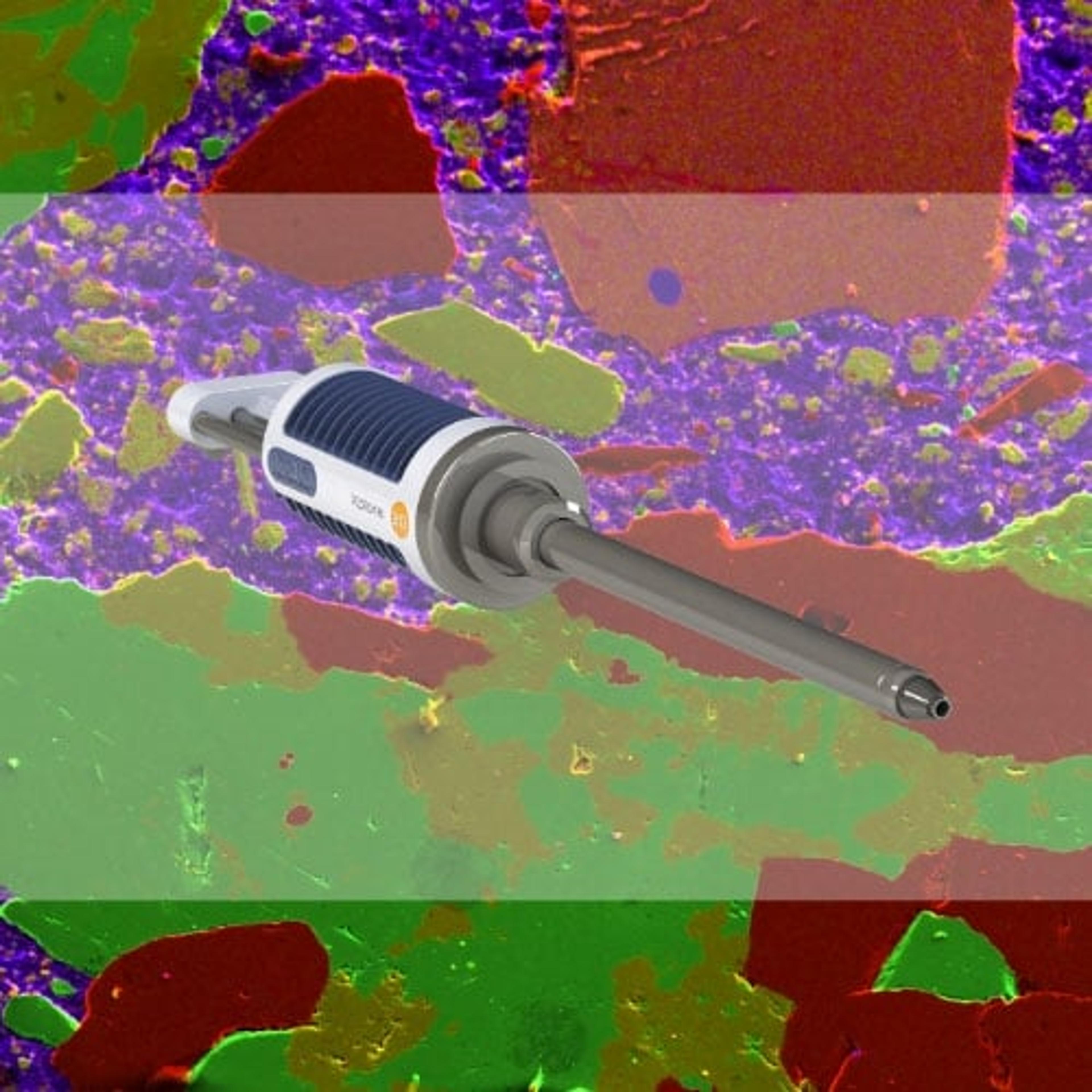
Rapid characterization of steel and nickel
In this application note, Oxford Instruments NanoAnalysis gives examples of how Symmetry can be used to characterize the microstructures in two example metals, at high speeds, providing reliable statistics in affordable timescales.

From niche to mainstream: why EBSD has become a routine technique for materials characterisation
Electron backscatter diffraction (EBSD) in scanning electron microscopes is a surface analysis technique that has been commercially available for over three decades. However, only in recent years has it become a well-established tool for routine materials characterization. In this webinar, following a general overview of the technique, we will look at the recent developments, from faster detectors to more automated software, that have enabled the transition of EBSD into a mainstream analytical method. Finally, we will assess the latest advances in EBSD technology and show how these are opening up new application fields, from biomaterials to batteries.
Key learning objectives
- Develop a broad understanding of the EBSD technique
- Gain knowledge about the type of information provided by EBSD analyses
- Consider how recent developments have made EBSD faster and more versatile
- Understand new ways in which EBSD is solving problems in diverse application fields
Who should attend?
- Students learning about material characterization methods
- Existing users of EBSD interested in recent advances
- Scientists in any field that involves crystalline materials, such as materials science, microelectronics, biomaterials, or the Earth and planetary sciences

Materials science: Key technological advancements to celebrate

Electron backscatter diffraction: Moving toward the mainstream for crystalline material characterization
Dr. Pat Trimby reveals the innovations that have transformed EBSD from a specialized method to a workhorse for routine material analysis