Electron backscatter diffraction: Moving toward the mainstream for crystalline material characterization
Dr. Pat Trimby reveals the innovations that have transformed EBSD from a specialized method to a workhorse for routine material analysis
24 May 2023

Electron backscatter diffraction (EBSD) is a technique that employs scanning electron microscopy to examine, visualize, and measure the microstructure of a sample. While commercial EBSD systems have been around since the 1990s, the technique was initially slow to take off due to its perceived complexity, lengthy analysis times, and limited range of applications. However, in the past decade, EBSD systems have undergone significant improvement. Advancements in detector technology have increased the analysis speed by tenfold, while software developments have opened the approach to non-expert users and extended its utility across diverse research fields, such as biomaterials and green energy research.
In this article, SelectScience® speaks with Dr. Pat Trimby, EBSD Product Manager at Oxford Instruments, to learn more about the latest iteration of EBSD systems and how they are designed to meet the demands of routine crystalline material characterization. Trimby also discusses some of the latest applications of EBSD and highlights resources available to help researchers learn more about the principles, benefits, and practical application of this powerful approach.
How does EBSD work?
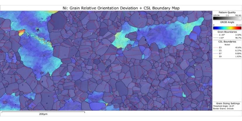
Electron backscatter diffraction is a scanning electron microscope (SEM) based technique that involves directing a stationary electron beam on a tilted crystalline sample. The electron beam interacts with the sample and scatters off its surface, forming a distinctive pattern that can be captured with a fluorescent screen positioned at the end of a detector. The diffraction pattern is indicative of the crystal structure and orientation at the point where the electron beam interacts with the sample and hence can be used to discriminate between different phases, characterize grain sizes and boundaries, and determine the preferred crystal orientation within the sample, known as its texture. By scanning the electron beam in a grid pattern across the sample's surface, a complete and quantitative map of the microstructure can therefore be obtained (Fig.1.).
An era of innovation
The two primary components of any EBSD system are its detector and processing software, which together enable diffraction patterns to be collected, indexed, and analyzed for interpretation. Advancements in detector technology have been the driving force behind the most significant developments in EBSD. According to Trimby, one of the biggest changes came from the introduction of high-speed complementary metal oxide semiconductor (CMOS) technology, led by the launch of the Oxford Instruments Symmetry® EBSD detector in 2017.
“Until that stage, all EBSD detectors were using charge-coupled device (CCD) sensors, which were good, but if you wanted to collect your diffraction patterns quickly, you needed to downsize the images using pixel binning,” explains Trimby, noting that by grouping pixels in this way, patterns could be acquired at greater speeds but at the expense of reduced resolution and dynamic range.
In contrast to CCD sensors, CMOS sensors have a more parallel architecture and can read out higher resolution images at high speeds. “We could go from working at 1,000 patterns per second to 3,000–4,000 patterns just by switching to CMOS technology,” Trimby adds. “We're now at 5,000–6,000 analyses per second and what used to take many hours, we can now do in a matter of minutes. This has really changed the way people are using EBSD, and for many, it has become a routine characterization technique.”
Improvements in detector technology have been complemented by advancements in data processing and analysis capabilities. “These have been driven not only by the development of new code by researchers on open-source platforms but also by the increasing integration of machine learning and artificial intelligence,” explains Trimby. “New sophisticated pattern-matching techniques have enabled the extraction of previously inaccessible information from diffraction patterns, and these are starting to expand the applications of EBSD.”
In the past, acquiring and processing rich EBSD datasets was a task that demanded a high level of expertise. However, with these recent advancements in both hardware and software, the process has become much more accessible. “It is now relatively easy to obtain high-quality data from samples, and some of the processes that were previously reserved for experts are now semi- or fully automated,” says Trimby. “There are still parts of EBSD that remain quite difficult, but it's much, much easier than it used to be.”
Comprehensive characterization with broad application
According to Trimby, one of the key benefits of EBSD is its ability to be paired with energy-dispersive X-ray spectrometry (EDS), allowing the near-complete characterization of samples at a high resolution. “By integrating EBSD and EDS measurements, we can resolve details of a sample’s chemistry and structure down to the tens of nanometers scale, and covering hundreds of microns or even millimeters across the surface of the sample,” he adds.
The combination of EBSD and EDS allows for the comprehensive analysis of a sample's composition, elemental distribution, phases, grain size, grain structure, boundaries, texture and local strain variation. These characteristics collectively determine the physical properties of the sample and are relevant to a wide range of industries and research areas, from metals research to advanced manufacturing techniques, renewable energy, microelectronics, and geological research. “It’s that all-encompassing characterization and the speed at which it can be achieved that makes EBSD-EDS an attractive technique for a growing number of fields,” explains Trimby.
One of the areas in which EBSD is gaining increasing utility is for the analysis of biomaterials, where improvements in detector sensitivity have opened the technique to samples that traditionally produced poor-quality diffraction patterns or are sensitive to damage by the electron beam. “This includes biomineralized materials, such as shell structures, where researchers are using EBSD to understand how particular biomineralized structures have evolved,” says Trimby. “We also see similar applications in organic thin films, such as thin-film solar cells, and this is very important for solar cell technology.”
A dedicated EBSD learning center
For researchers looking to expand their knowledge and competency of EBSD, Oxford Instruments has a dedicated website, EBSD.com. Split into two parts, the website offers a wealth of information and guidance for individuals with varying levels of expertise in EBSD, ranging from newcomers to experienced users who want to explore advanced EBSD functions and new ways of interpreting EBSD data. “The first part offers an overview of the technique's background, how EBSD works, the different techniques for EBSD analysis, and the different ways people are applying this method,” explains Trimby. “The second part offers more practical assistance to users, such as guidance on sample preparation, optimal sample setup in the microscope, and information about using the advanced features of the Oxford Instruments EBSD hardware and software. The website also contains numerous instructional videos, tutorials, and blogs to help users get the most out of their EBSD system.”
Future outlooks
EBSD is a constantly evolving technique with new applications emerging almost every month. Looking ahead, Trimby notes that further improvements to EBSD analysis speeds may be capped by the availability of electrons in SEM, however, he expects to see the emergence of new sampling strategies. “For example, smart sampling or compressed sensing, where we don't need to analyze every pixel in our detector to be able to get the relevant information,” he says. While re-emphasizing the increasing role of AI and machine learning in processing EBSD data, Trimby suggests that the most significant developments in EBSD lie in enhancing its ease of use. “EBSD software is starting to develop a degree of intelligence and we will see that progressing in the coming years,” he says. “Ultimately, this will open the door even wider for non-experts to harness the power of EBSD,” he concludes.
Find out more about EBSD in this exclusive webinar with Dr. Pat Trimby >>
Related Products
Request Quote for All Products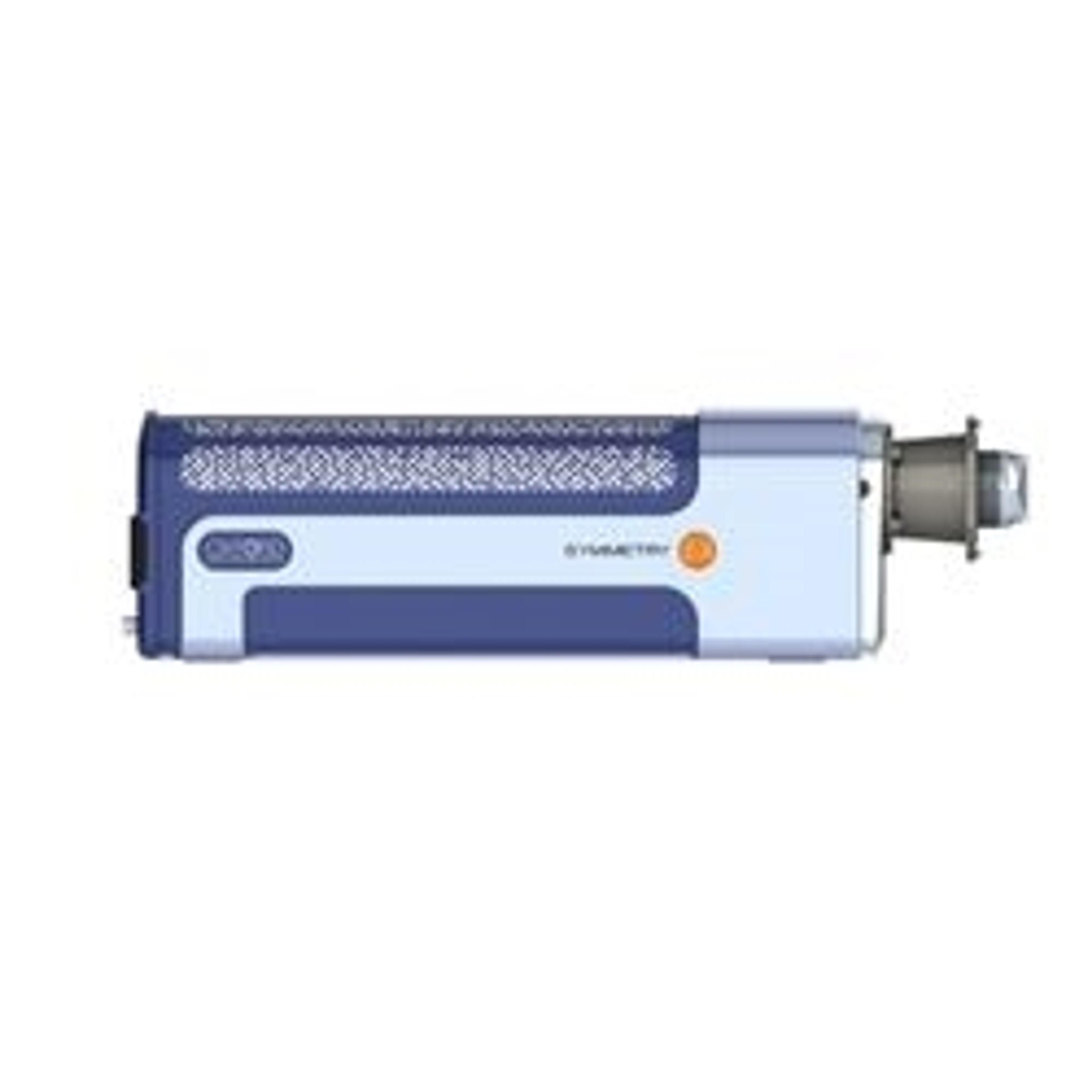
Symmetry® S3
Oxford InstrumentsThe Symmetry S3 is the only genuine all-in-one EBSD detector on the market, and is based on the revolutionary Symmetry detector, the world’s first EBSD detector to utilise advanced CMOS technology.