ResourceLab Automation
Semiconductor mapping in transmission electron microscopy
23 Aug 2019Elemental analysis of semiconductors is typically difficult due to strong overlaps of X-ray lines between commonly used elements and low concentrations of dopants. Not only are concentrations of dopants small but their X-ray lines often overlap with other materials used in semiconductor processing. In this application note, Oxford Instruments NanoAnalysis shows how AZtecTEM solves these overlaps to achieve an accurate elemental analysis.
Related Products
Request Quote for All Products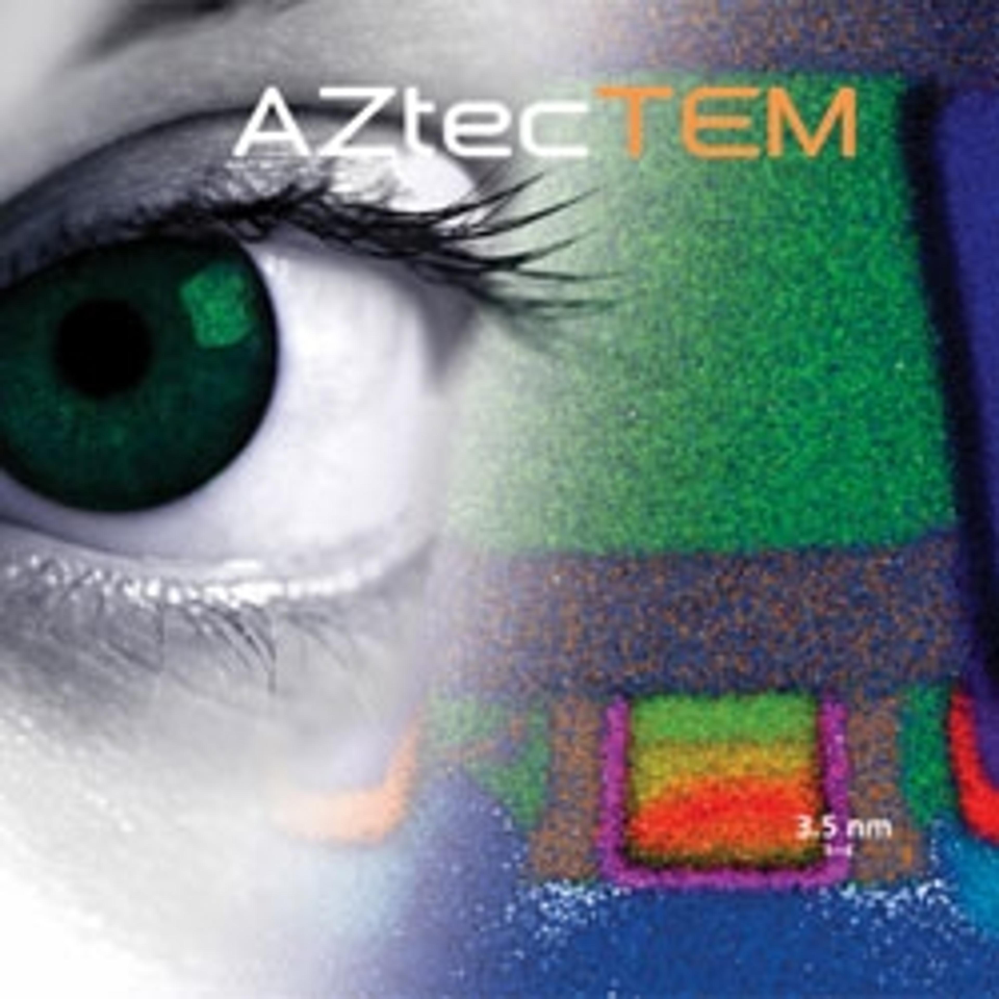
Ultim® Max and AZtecTEM
Oxford InstrumentsAZtecTEM, powered by Ultim™ Max (Silicon Drift Detector), provides exceptional elemental characterisation abilities in the TEM.