Materials science is a multidisciplinary field that enables us to better understand and explore the properties of a given material at the micro- and nanometer scaled level – by applying physics, chemistry, mathematics, and engineering. Over the past few decades, there have been significant advances in the field of materials science, which has led to the development of many novel materials, e.g. nanomaterials such as the well-known graphene, with remarkable properties and applications. The discovery and development of new materials mean that we can improve how to detect disease, build more sophisticated instruments, and lead more efficient lives. The field of materials science has had a profound impact on society, and it is difficult to imagine a single aspect of daily life without it. From the clothes we wear to the smartphones and watches we use - materials science plays a critical role in shaping the way we live.
The recent advances in materials science have led to the development of more energy efficient solar panels, batteries, coatings, nanotubes, and semiconductors. Nevertheless, the demand for more effective and faster tools continues to grow. This is why materials science will remain at the forefront of science - to ensure that we keep up with the ever-increasing pace of modern life.
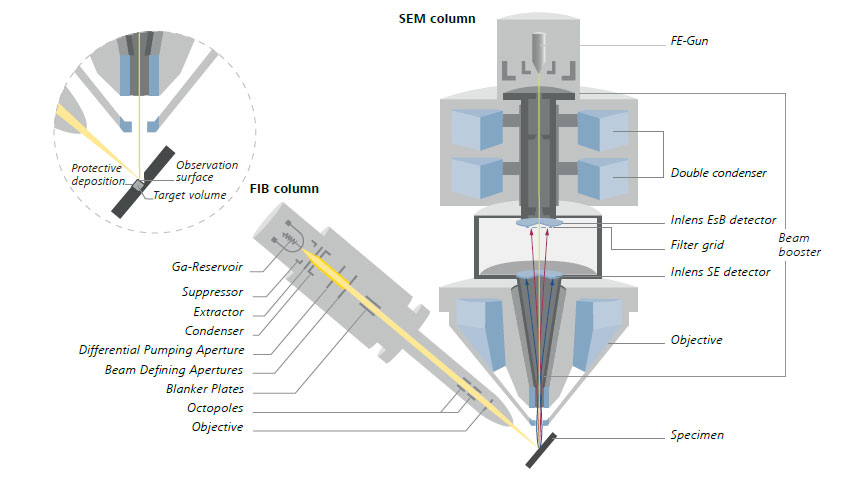
Microscopy has become an indispensable tool that has helped to advance the field of materials science, especially in nanotechnology. Microscopic imaging and analytical techniques play a crucial role in materials science by allowing researchers to effectively visualize and analyze the micro- and nanometer scaled structure and overall properties of a range of materials. These simple, yet powerful tools, enable researchers to explore the strength, structure, conductivity, and optical properties of a material, along with many other vital components. There are many types of microscopes available on the market, some of the most relevant for advancing materials science being scanning electron microscopy (SEM), focused ion beam-scanning electron microscopy (FIB-SEM), X-ray microscopy (XRM), and related preparation, testing and analytical methods such as micro- and nanomachining, in situ testing or energy dispersive spectroscopy (EDS). Each of these techniques have their own strengths and limitations, but all provide valuable information.
One of the main advantages of microscopy is the ability to provide high-resolution images. The generation of high-resolution images means that researchers can explore and investigate a given material like never before, including defects and how a material behaves in situ – under high pressure or temperature or over time. By observing how a material behaves in all conditions, we can then determine how a material will behave in real-world situations, which is a vital component for how we develop new tools, such as batteries with longer lifetimes or point-of-care diagnostics.
Revolutionizing microscopy with ZEISS
ZEISS and its team of scientific experts are passionate about microscopy and continue to develop innovative microscopy solutions to move the field to new heights. ZEISS has now established itself as a leading provider of cutting-edge microscopic tools, designed to enable both academic researchers and industries to enable the advancement of materials science. ZEISS solutions cover a broad range of microscopic techniques, including scanning electron microscopy (SEM), focused ion beam-scanning electron microscopy (FIB-SEM), and X-ray microscopy (XRM), among many others. These solutions not only facilitate new discoveries, but they also provide valuable insights into the micro-and nanostructure of all materials.
ZEISS also provides a range of services and support to help users gain the most out of their systems. This includes training, maintenance, and technical support to ensure that researchers and industries can continue to advance their research, make new discoveries, and pave the way for future innovations.
Microscopy is an essential tool that is routinely used in materials science research. It is vital that researchers choose the right microscopy solution for their work and unique needs. By choosing the right solution, users can gain insights into the structure, function, and behavior of a given material to help them answer critical questions and advance their understanding of the material.
Since there are a whole range of different microscopes available on the market, it is crucial the end user understands which solution to choose. For instance, optical microscopy, electron microscopy, and X-ray microscopy all offer different advantages and limitations – in terms of spatial resolution, contrast, and sample preparation requirements. Optical microscopy is a common choice for those choosing to investigate the surface morphology and grain structure of a material. Alternatively, scanning electron microscopy provides higher resolution and magnification, allowing for the visualization of not only of micro- but also of nano-scaled features, such as defects within graphene. XRM and FIB-SEM expand the accessible information from 2D into 3D enabling the investigation of a three-dimensional volume instead of a two-dimensional surface only.
By selecting the most appropriate microscopy solution for a unique research need, scientists can improve the quality and accuracy of their data, increase the speed and efficiency of their experiments, and achieve more meaningful results. Additionally, choosing the right microscope can help researchers save time and money by avoiding unnecessary equipment purchases. Therefore, it is essential to consider the sample type, size, and features, as well as the research objectives, before choosing the appropriate microscopy solution.
In the free resources below, we explore:
FE-SEM
In FE-SEM a sample is scanned with a focused electron beam point by point (also known as “raster”) to obtain images with information about the samples’ topography and material composition.
Analytics
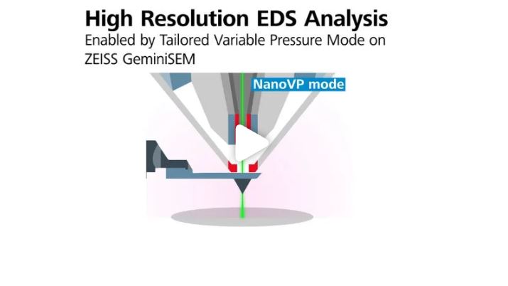
FE-SEM or FIB-SEM instruments can be equipped with analytical accessories. Complement the information you extract from your images with more knowledge on chemical composition using EDS, Raman spectroscopy, secondary ion mass spectrometry (SIMS) or crystallography (EBSD) of your sample.
FIB-SEM
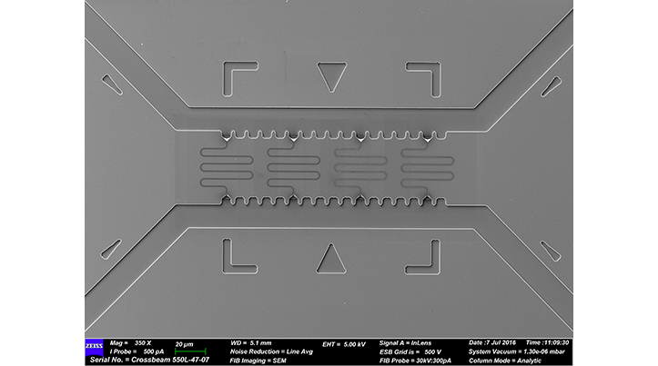
FIB-SEM can be used to speed up nanotomography and nanofabrication applications. Combine the imaging and analytical performance of high-resolution FE-SEM with the processing ability of a focused ion beam (FIB).
Software for connected microscopy or AI-based processing
Connect multiple length scales or microscopic and analytical modalities with each other by using solutions tailored for correlative microscopy. Benefit from relocating regions of interest over modalities, large area imaging or overlay image and analytical results. Use artificial intelligence-based algorithms like deep learning or machine learning for image segmentation, object classification, or batch processing.
Download
Download
Download
Download
Watch video
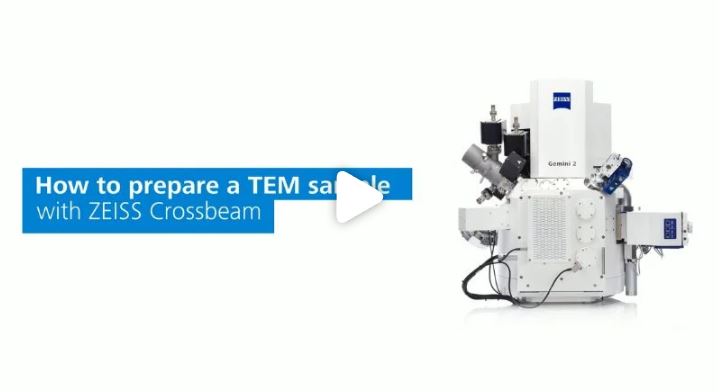
To gain a deeper understanding of ZEISS technology and its diverse applications, explore the following free resources below. These resources include detailed information on how to effectively set-up a ZEISS FIB-SEM system, along with a collection of informative videos focused on the features of the Crossbeam laser, transmission electron microscopy (TEM) sample prep tips, and how to achieve high-resolution EDS analysis.
Periodic Table of the Elements with Isotope Mass and Abundance
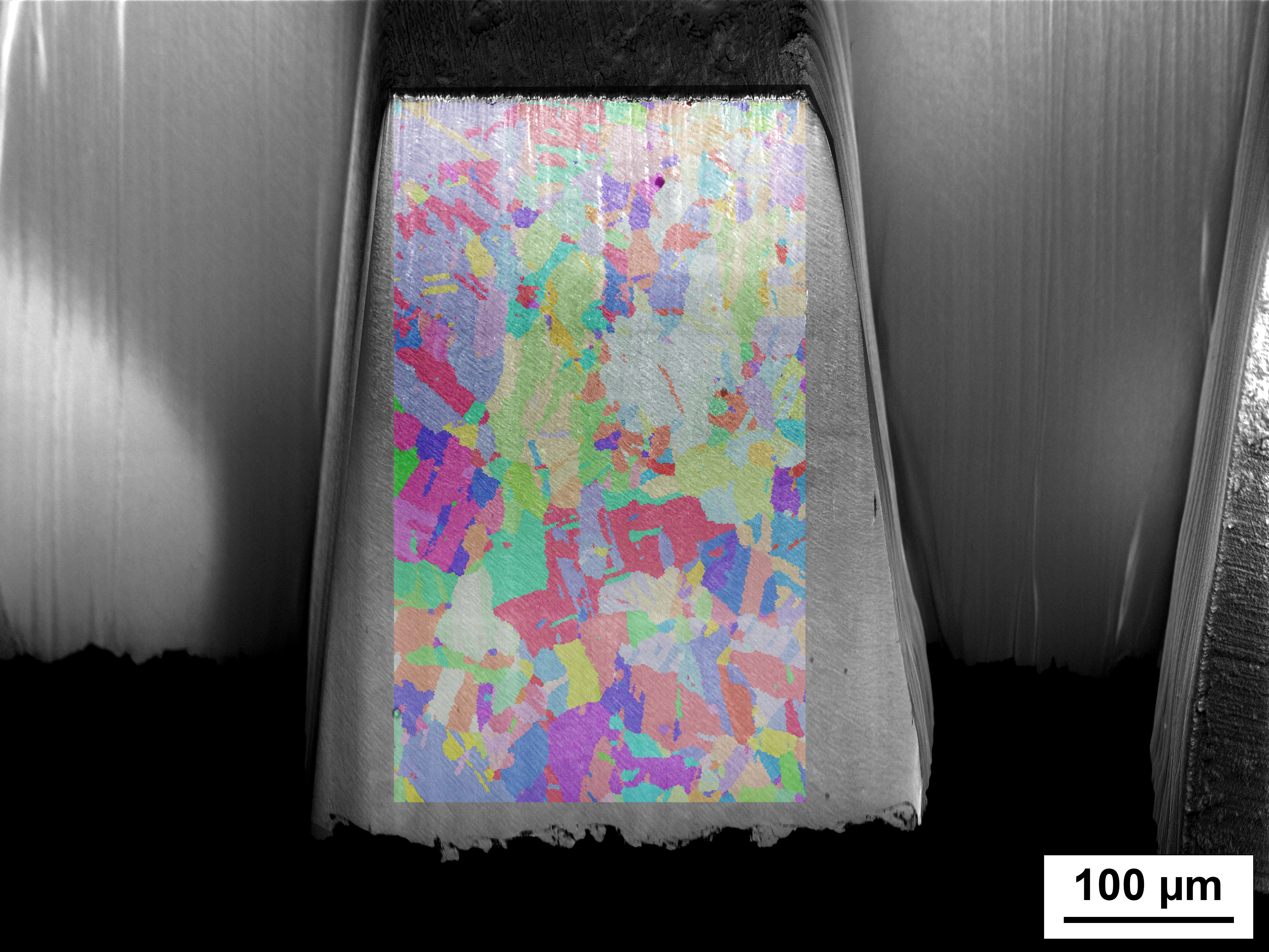
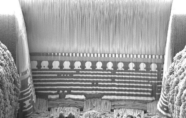
Electron backscatter diffraction (EBSD) is a scanning electron microscope based technique used throughout the field of materials science and is used to study the crystallographic structure of a material at the microscopic level.
This powerful technique involves using an electron beam to directly interact with a sample, and follows on by analyzing the diffraction patterns that are produced by the backscattered electrons. During an EBSD measurement, the sample is first prepared by polishing it to a smooth surface, before it is subjected to electron beam bombardment. Once this is complete, the backscattered electrons are collected by a detector, and the diffraction pattern produced by the backscattered electrons is analyzed to determine the crystallographic structure of the material.
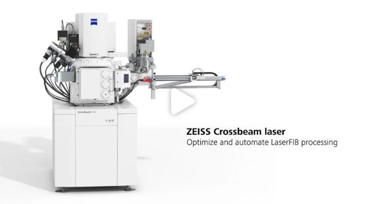
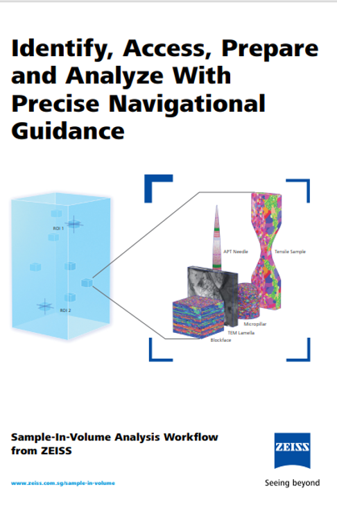
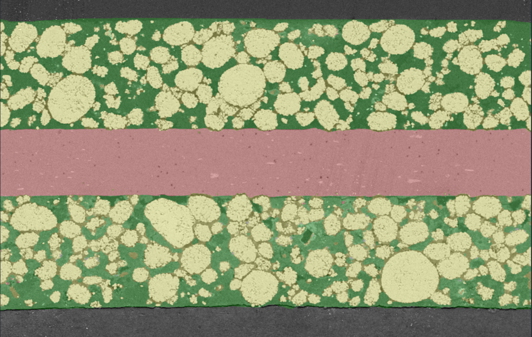
Sample preparation performed by FIB-SEM provides location-specific cross-sectioning while maintaining a virtually deformation-free microstructure. It is possible to prepare cross-sections that extend to several hundred micrometers in length and depth and thus provide better statistics in microstructure characterization. However, this has shown to be a time and cost intensive method. To overcome said issues, femtosecond laser ablation systems were implemented in ZEISS FIB-SEM systems. The use of a femtosecond laser facilitates extremely fast sample machining and surface preparation and has also shown to enable EBSD analysis directly on the laser polished surface due to the pseudo athermal ablation process it provides.
For more information on this powerful tool, explore the resource below. This resource will also introduce the ZEISS Crossbeam laser and explain how it can be used to achieve a preparation quality that is suitable for direct EBSD measurement on a laser polished surface.
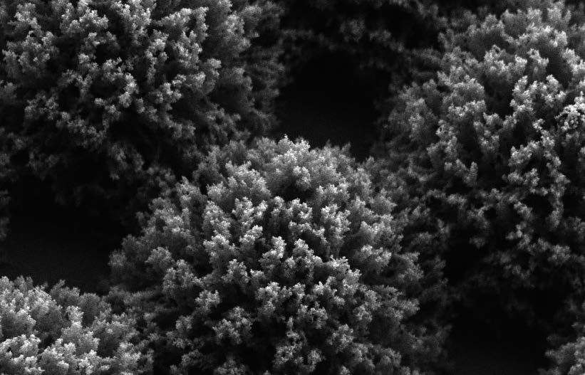
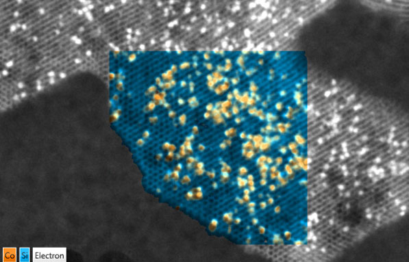
Accurately characterizing nanomaterials is crucial to produce precise results, especially considering their distinct properties and behavior, which can vary significantly from their bulk counterparts. These unique properties can include a high surface area-to-volume ratio, enhanced reactivity, and quantum confinement effects, among others.
Accurate characterization of nanomaterials is critical for understanding and controlling these unique properties and behavior, which is essential for the development and optimization of a wide range of applications. Plus, nanomaterials have the potential to interact with biological systems in ways that are not yet fully understood, so it is important to be able to accurately characterize these materials to assess their potential risks, such as in the field of nanotoxicology.
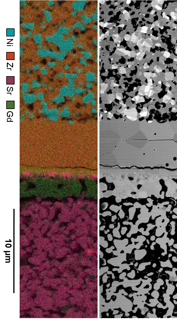
To find out more about the characterization of nanomaterials, explore the free resources below. These resources explore not only nanofibrous scaffolds for tissue engineering investigated by XRM, but also how graphene can be characterized via FE-SEM and Raman spectroscopy, and how nanofluidic devices are manufactured by FIB-SEM. Plus, these resources also explore how SIMS can help to advance nanoscience.
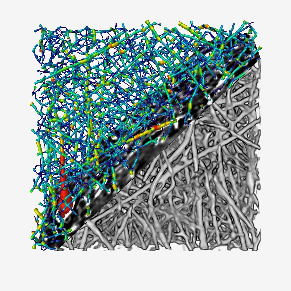
Characterization of the 3D Microstructure of Nanofibrous Scaffolds for Tissue Engineering
Download
In situ SEM and Raman Investigations on Graphene
Download
Fabrication and Characterization of Nanofluidic Devices for DNA Optical Mapping
Watch webinar
Nanoelectronics is a field of science and technology that deals with the study and application of electronic devices and systems - at the nanoscale level. Nanoelectronics is a rapidly growing field, with new discoveries and breakthroughs being made all the time.
At the nanoscale level, the properties of materials can be significantly different from those at the macroscopic level. These differences occur as a result of quantum mechanical effects, which may become more pronounced as the size of the material decreases. As a result of such differences in properties and behavior of nanomaterials, nanoelectronics has the potential to enable new technologies and applications that are not possible with traditional electronic devices, such as nanosensors and nanotransistors.
Fortunately, ZEISS microscopy solutions allow researchers and industries to solve pressing research challenges in electronics, cybersecurity, and quantum computing. For example, voltage contrast performed with FE-SEM enables defect analysis in electronic devices on a nanoscale. Artificial intelligence powered software solutions allow efficient, operator-independent microstructural analysis of lithium ion batteries based on batch segmentation of FE-SEM images. 3D volumes of solid oxide fuel cells can now be characterized with high-resolution imaging and EDS using 3D FIB-SEM tomography. To find out more, explore the resources below.
Characterization of Solid Oxide Electrolysis Cells by Advanced FIB-SEM Tomography
FE-SEM
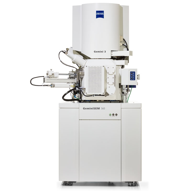
ZEISS GeminiSEM stands for effortless imaging with sub-nanometer resolution. Use it for your most demanding projects in materials and life science.
GeminiSEM
FIB-SEM (Crossbeam)
“Great product, essential to all our products; it never stands still in our lab!”
Silke Christiansen, Inam

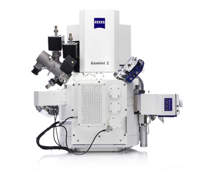
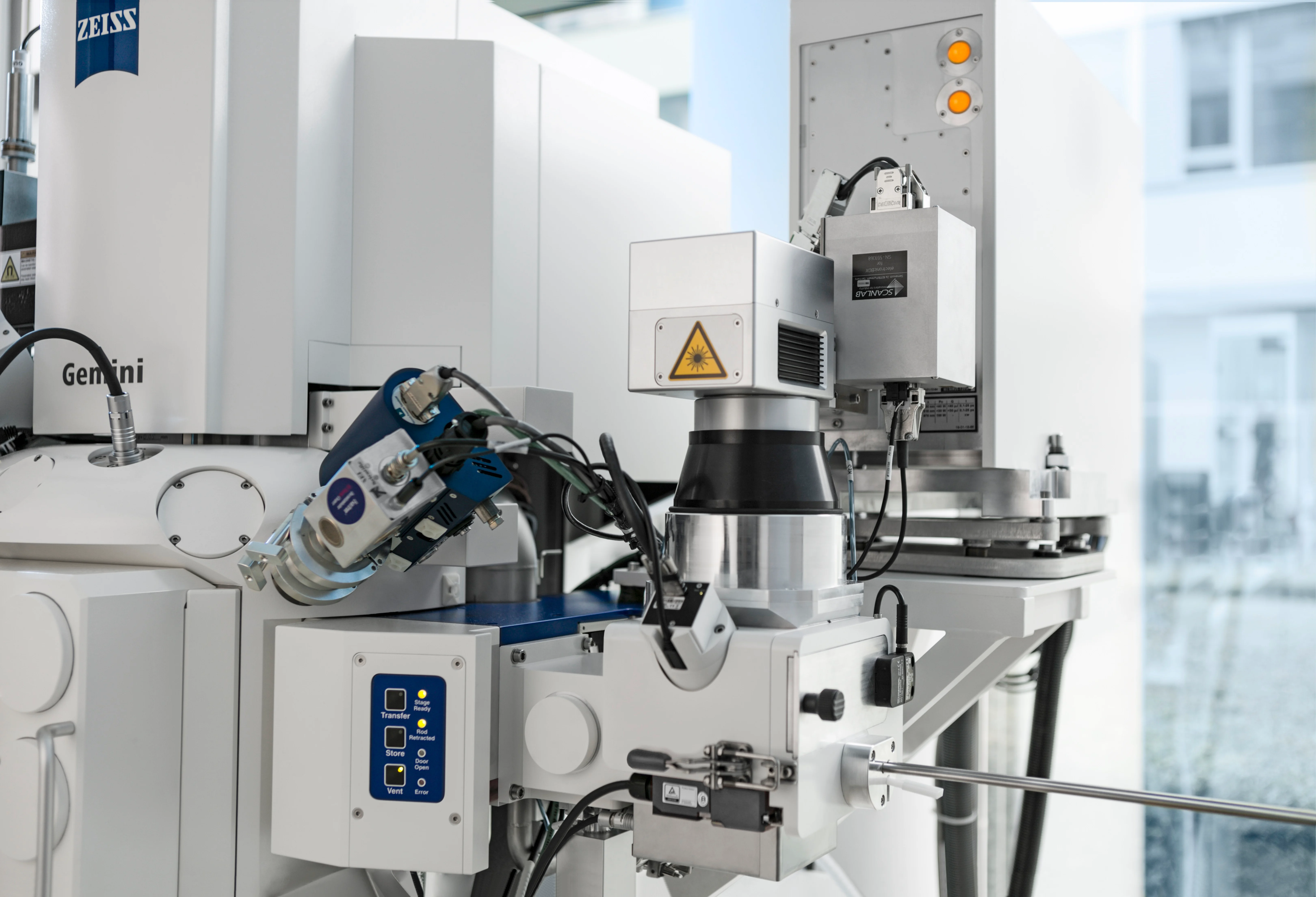
FIB-SEMs: (Crossbeam laser)
LaserFIB Workflow - Enhance Your in situ Studies.
XRM (Xradia Versa)
“Limitless opportunities to explore various unresolved domains in material science.”
Arun Torris, CSIR - National Chemical Laboratory
XRM (Xradia Ultra)
Your Ultra-high Resolution, Non-destructive 3D Imaging System.
Atlas 5
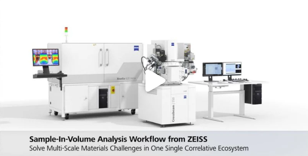
Create multi-scale, multi-modal images with a sample-centric correlative environment. Atlas 5 extends your ZEISS scanning electron microscopes (SEM) and focused ion beam SEMs (FIB-SEM). Efficiently navigate and correlate images from any source, e.g. light- and X-ray microscopes. Perform large area imaging, acquire nanoscale images, and correlate images in multiple dimensions from multiple sources.
ZEN core AI Toolkit
The AI Toolkit makes integrated, easy to use, powerful segmentation for 2D and 3D datasets available to routine microscopy users. It is a complete package for AI applications including integrated training interfaces
*Certain images and/or photos on this page are the copyrighted property of 123RF.com, its contributors or its licensed partners and are being used with permission under the relevant license. These images and/or photos may not be copied or downloaded without permission from 123RF.com. Other images courtesy of Zeiss®.