Characterization of Solid Oxide Electrolysis Cells by Advanced Focused Ion Beam-SEM Tomography
31 Jul 2017This white paper investigates the microstructural changes after cycling of a solid oxide electrolysis cell (SOEC), studied by means of focused ion beam (FIB)-SEM tomography. The advanced tomography package, ZEISS Atlas 5 3D Tomography, enables high-resolution 3D electron imaging and 3D energy dispersive X-ray spectroscopy (EDS) elemental imaging, using two different sets of SEM conditions optimized for the respective task.
Related products
Request Quote for All Products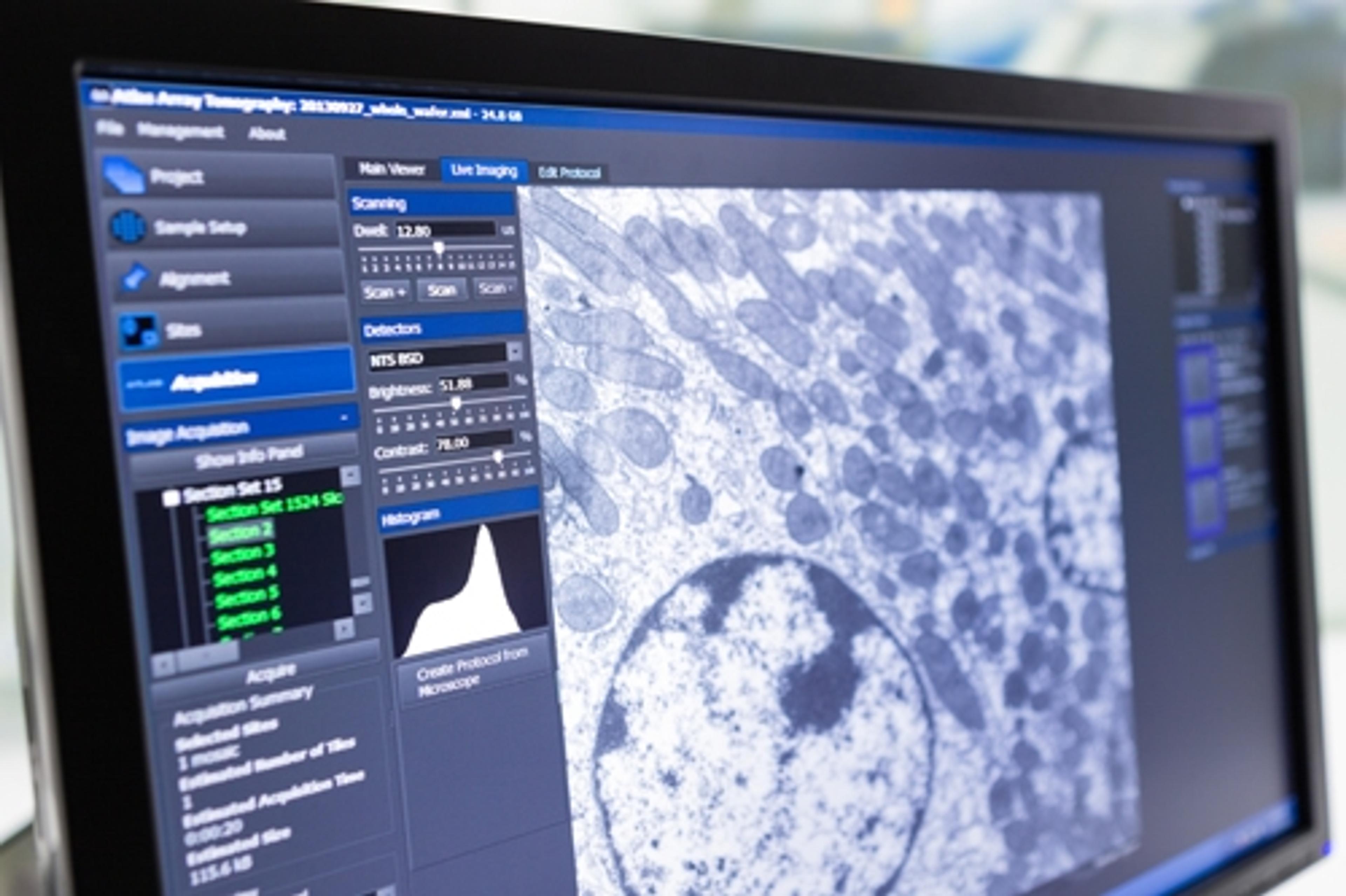
ZEISS Atlas 5
ZEISS Research Microscopy SolutionsLarge area imaging for SEM, FE-SEM & FIB-SEM ATLAS combines a 16 bit scan generator and dual super-sampling signal acquisition hardware with image processing and control software for your ZEISS electron microscope. Acquire images up to 32 k x 32 k pixels, with dwell times from 100 ns to > 100 s, adjustable in 100 ns increments. Save your images with eight or sixteen bits of intensity. With the ATLAS “Mosaic Tool” you create large image montages, automatically moving from image tile to tile, and mosaic site to site, resulting in an “Extreme Field of View” image, at SEM nanometer scale resolution. ATLAS provides • reduced number of tiles to acquire, reducing stage motion delay and areal fraction of each image “lost” to overlap • reduced number of overlap “seams”, leading to less beam damage and degradation of the sample • reduced computational complexity