Resources
25
Application eBook
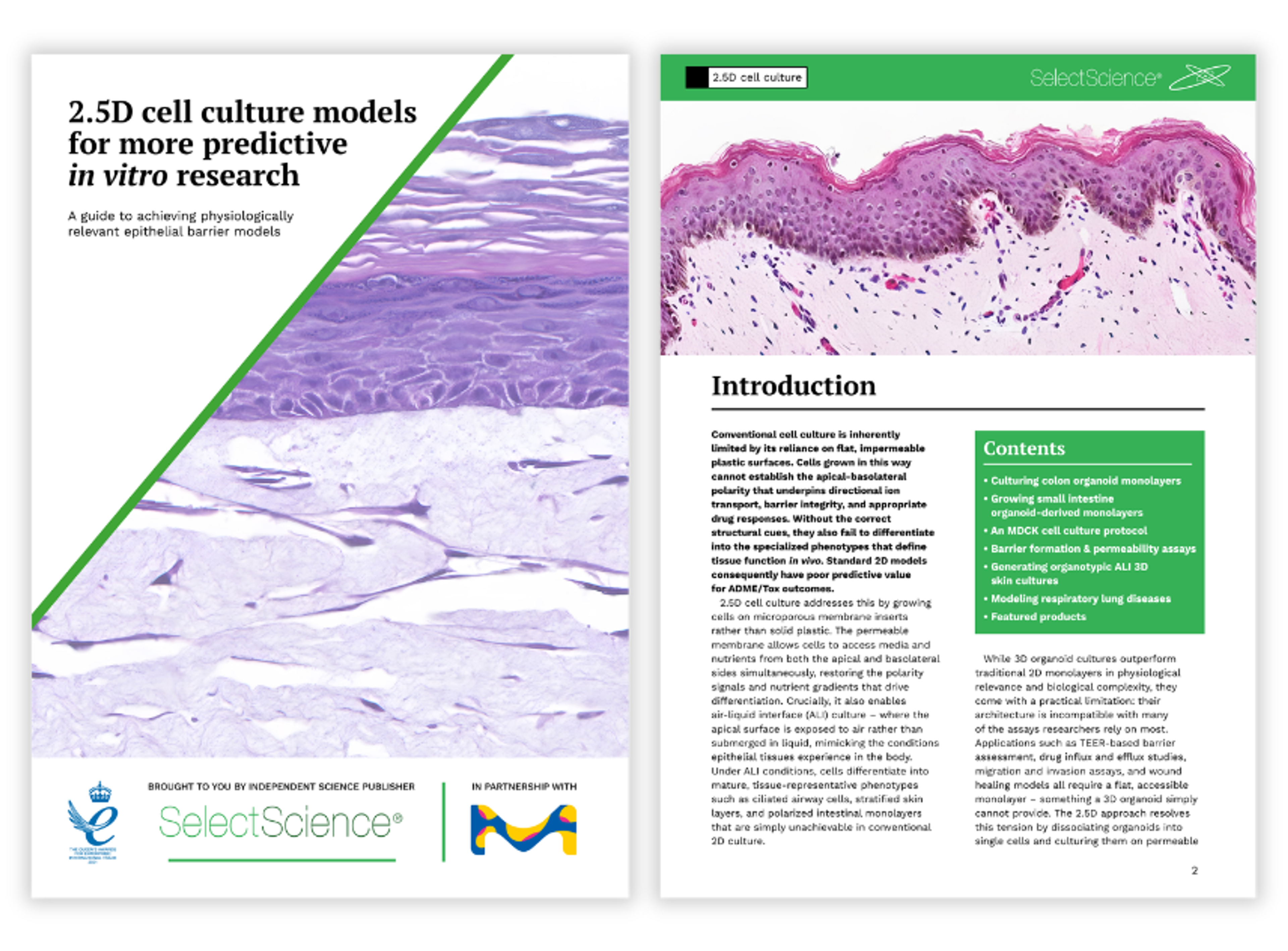
2.5D cell culture models for more predictive in vitro research
Product Brochures
Waters cloud software solutions
Application Note
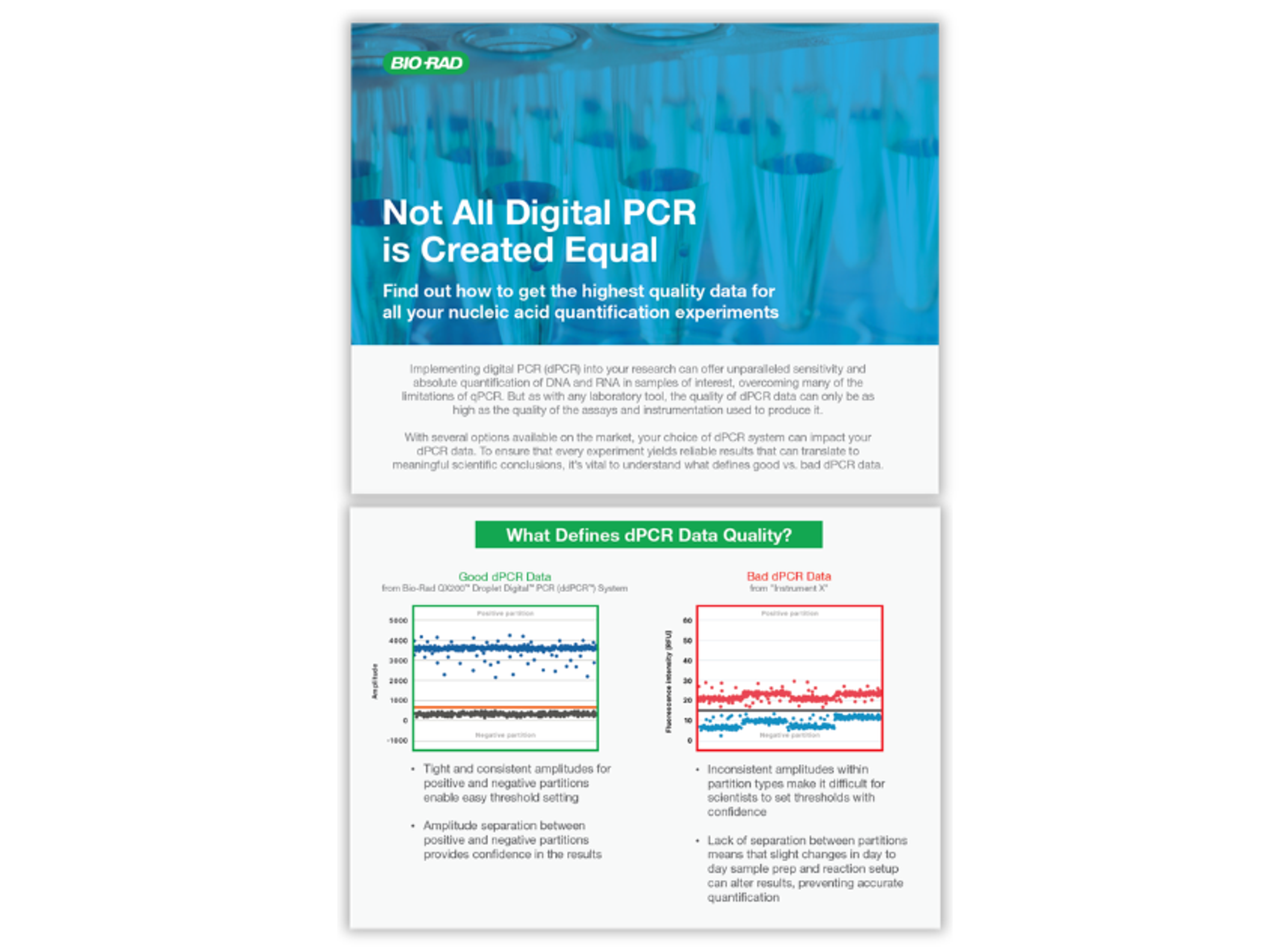
Not all digital PCR is created equal
Application Note
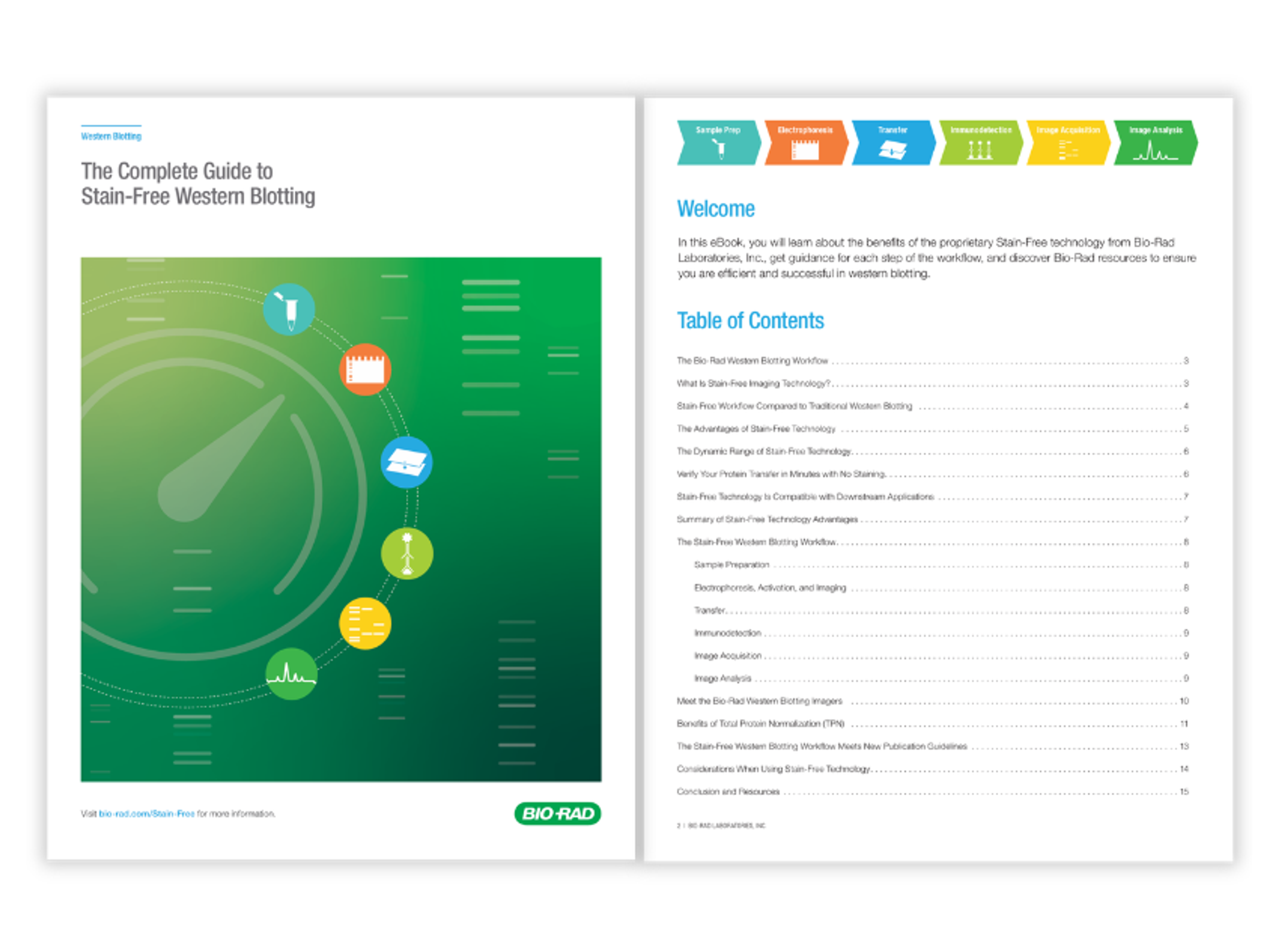
The complete guide to stain-free Western blotting
Application Note
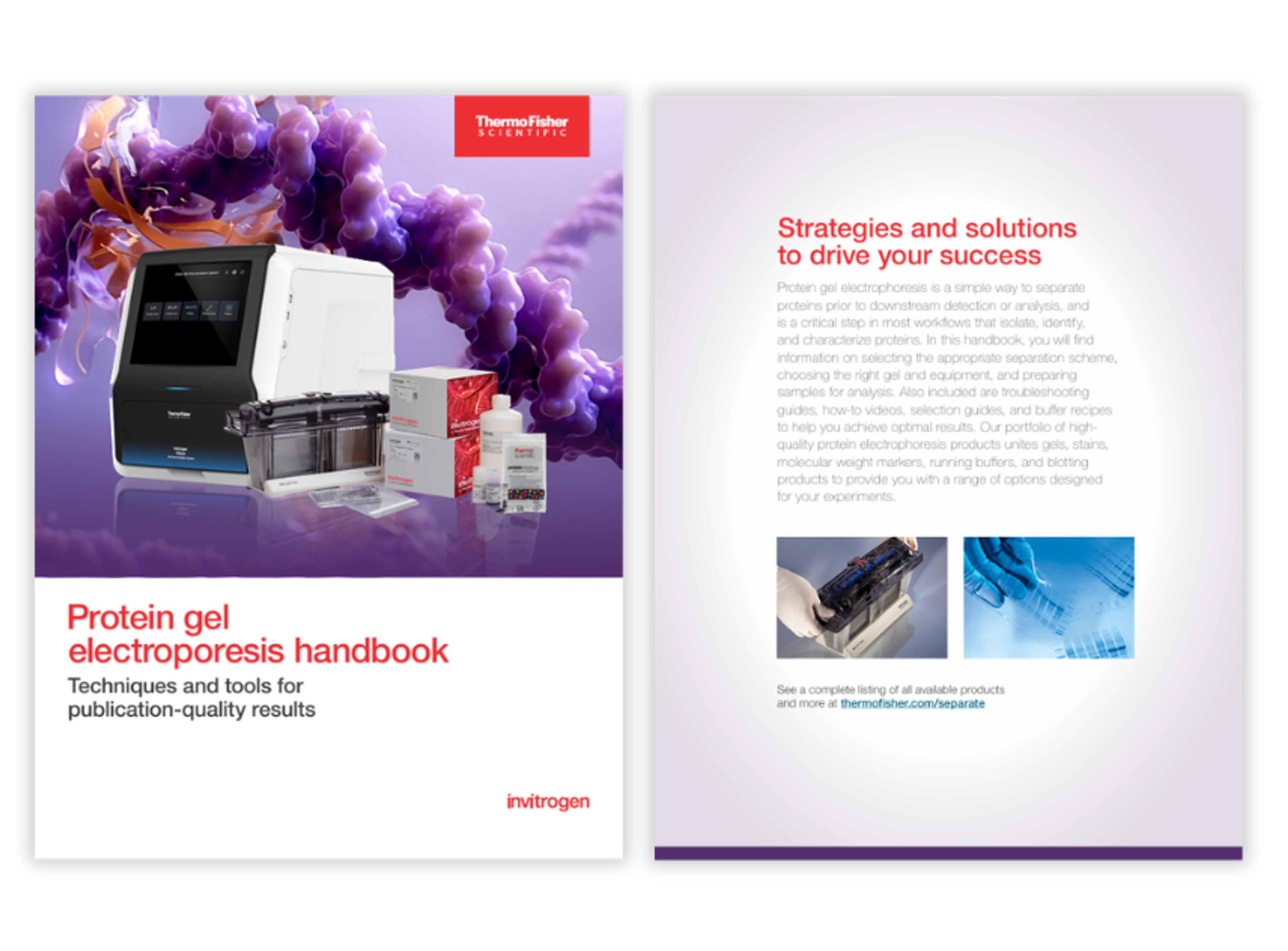
Protein gel electroporesis handbook
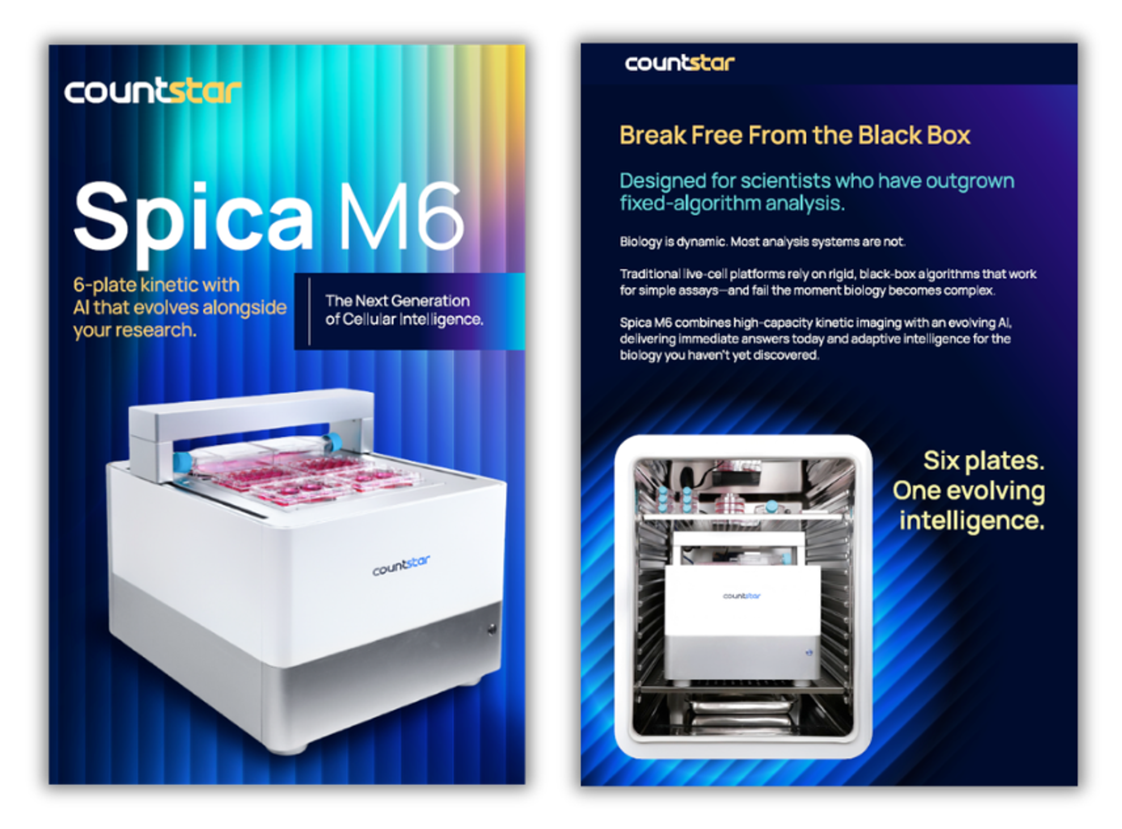
Product Brochures
Countstar Spica M6 brochure
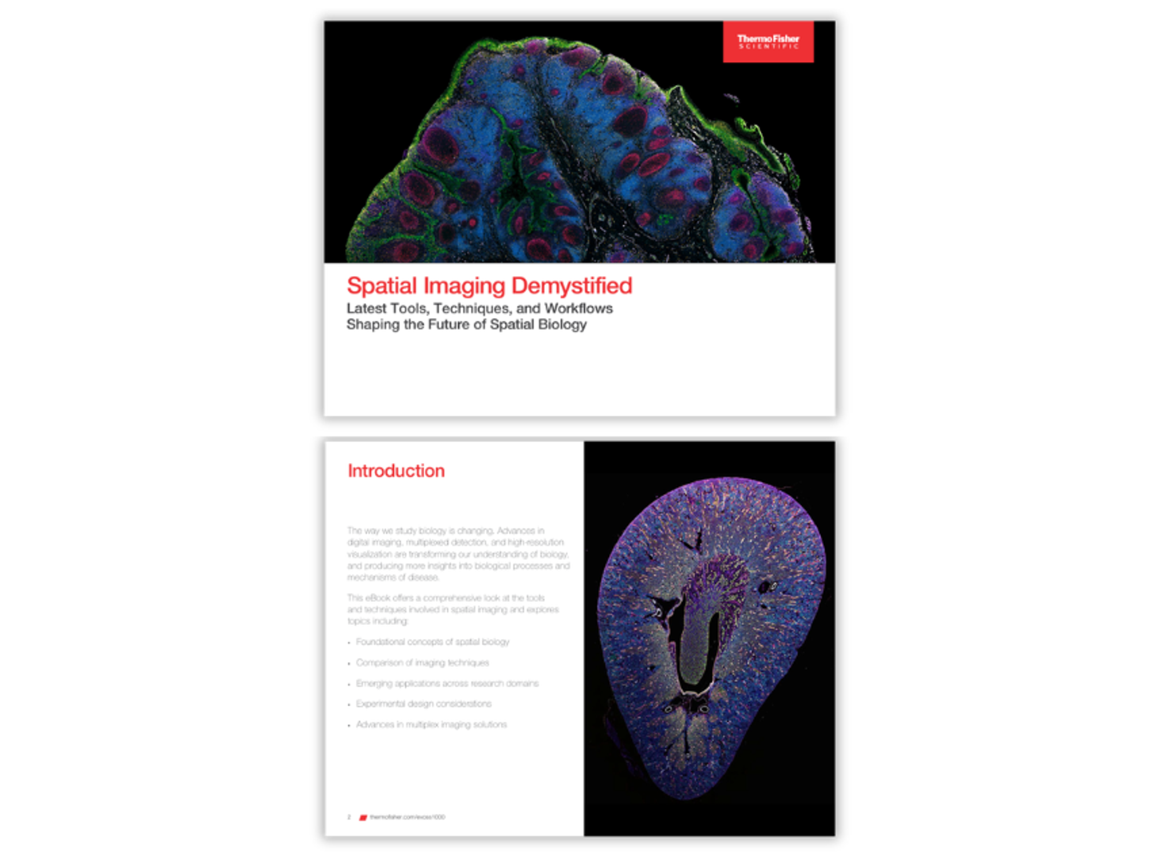
Application Note
Spatial imaging demystified
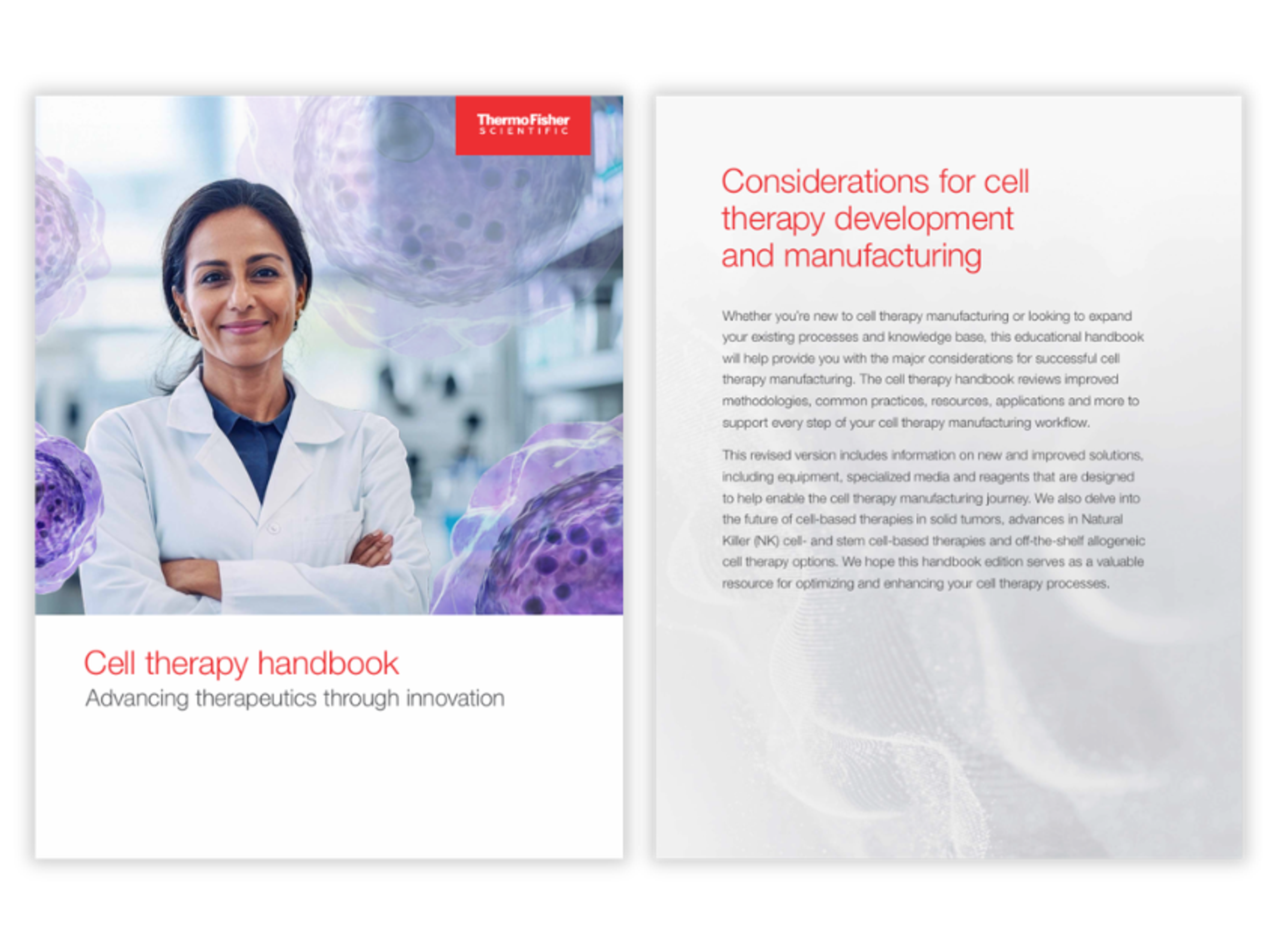
Application Note
Cell therapy handbook
Application Note