Resources
25
Application eBook
2.5D cell culture models for more predictive in vitro research
Application Note
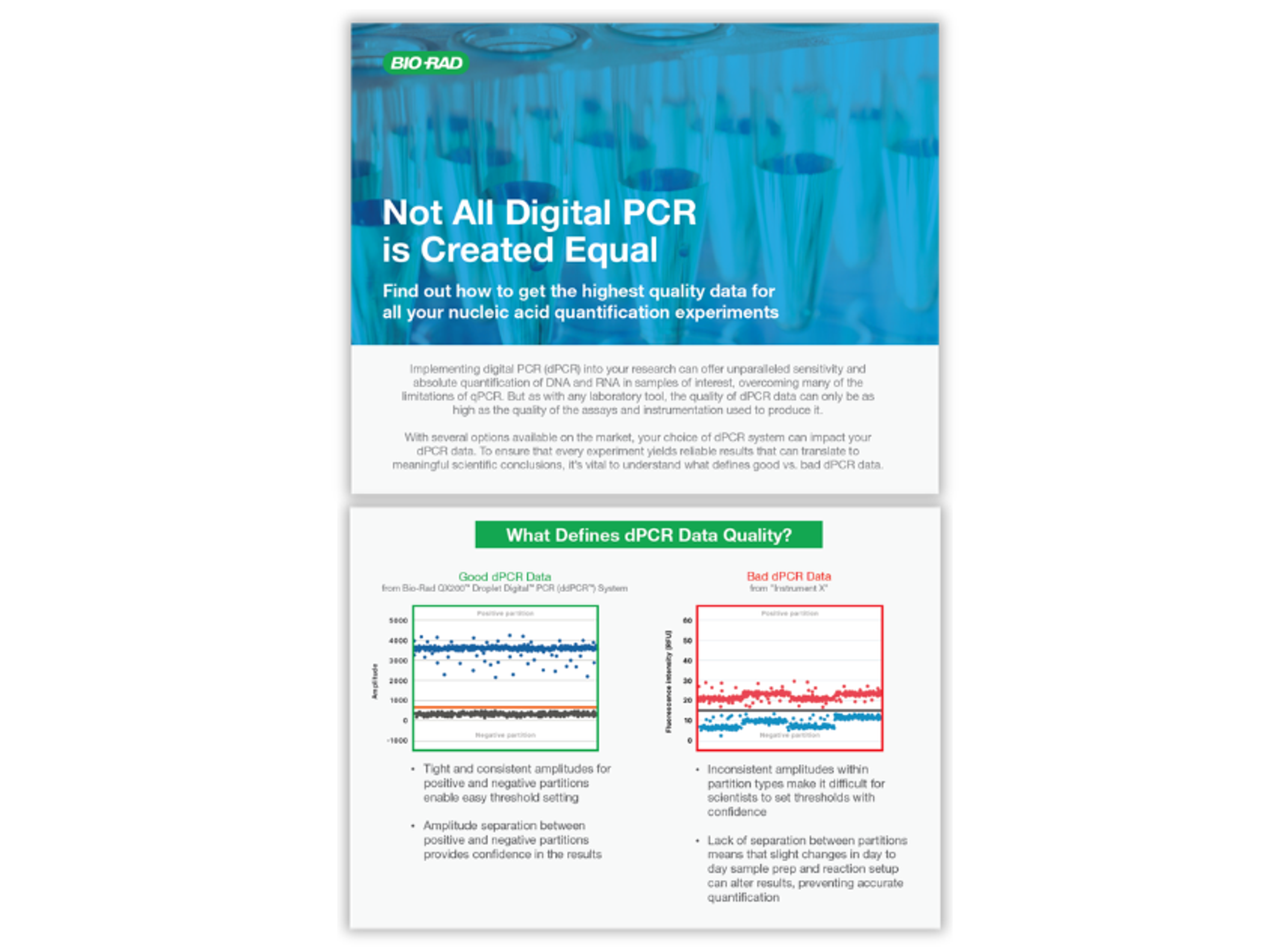
Not all digital PCR is created equal
Application Note
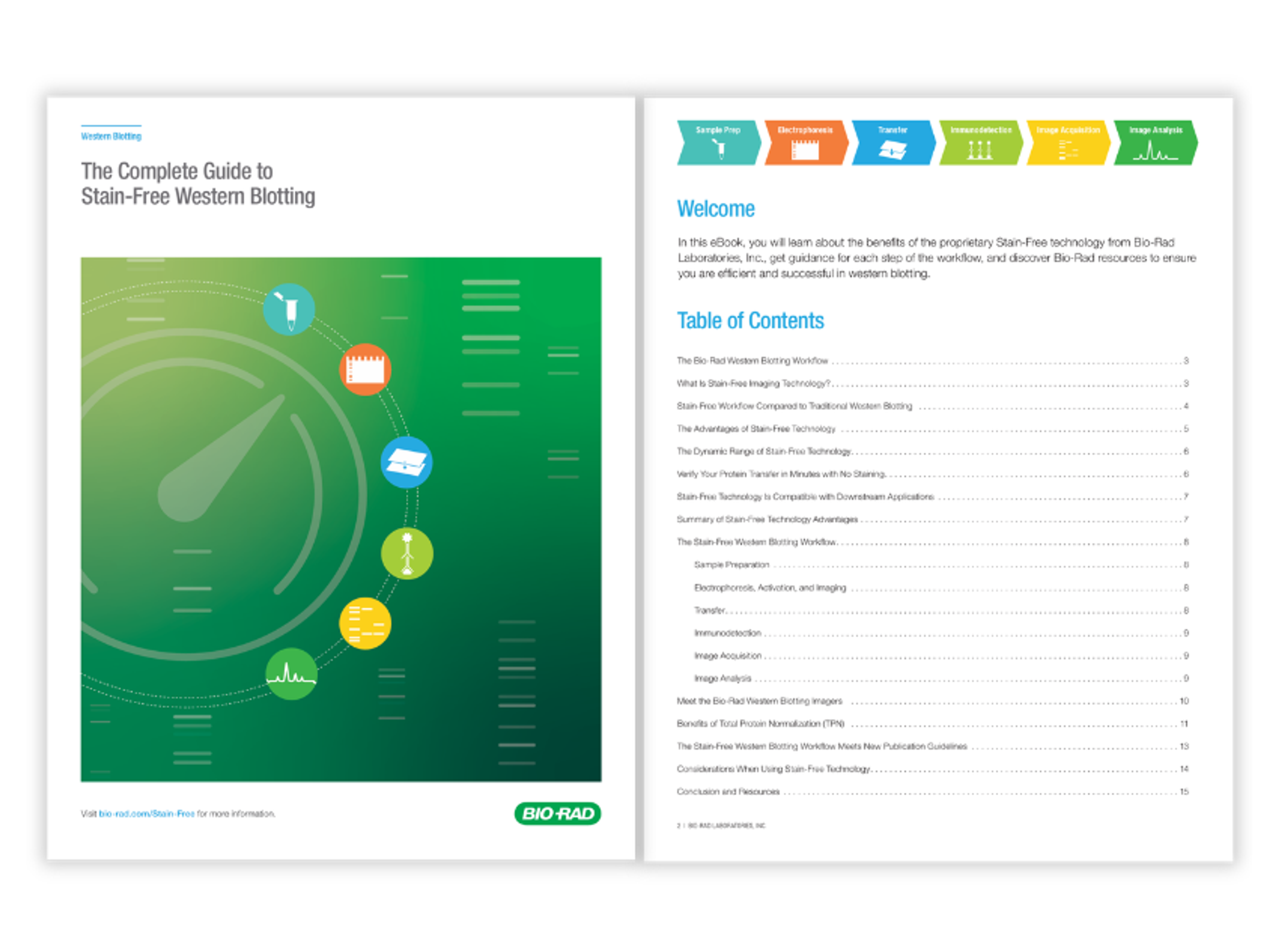
The complete guide to stain-free Western blotting
Application Note
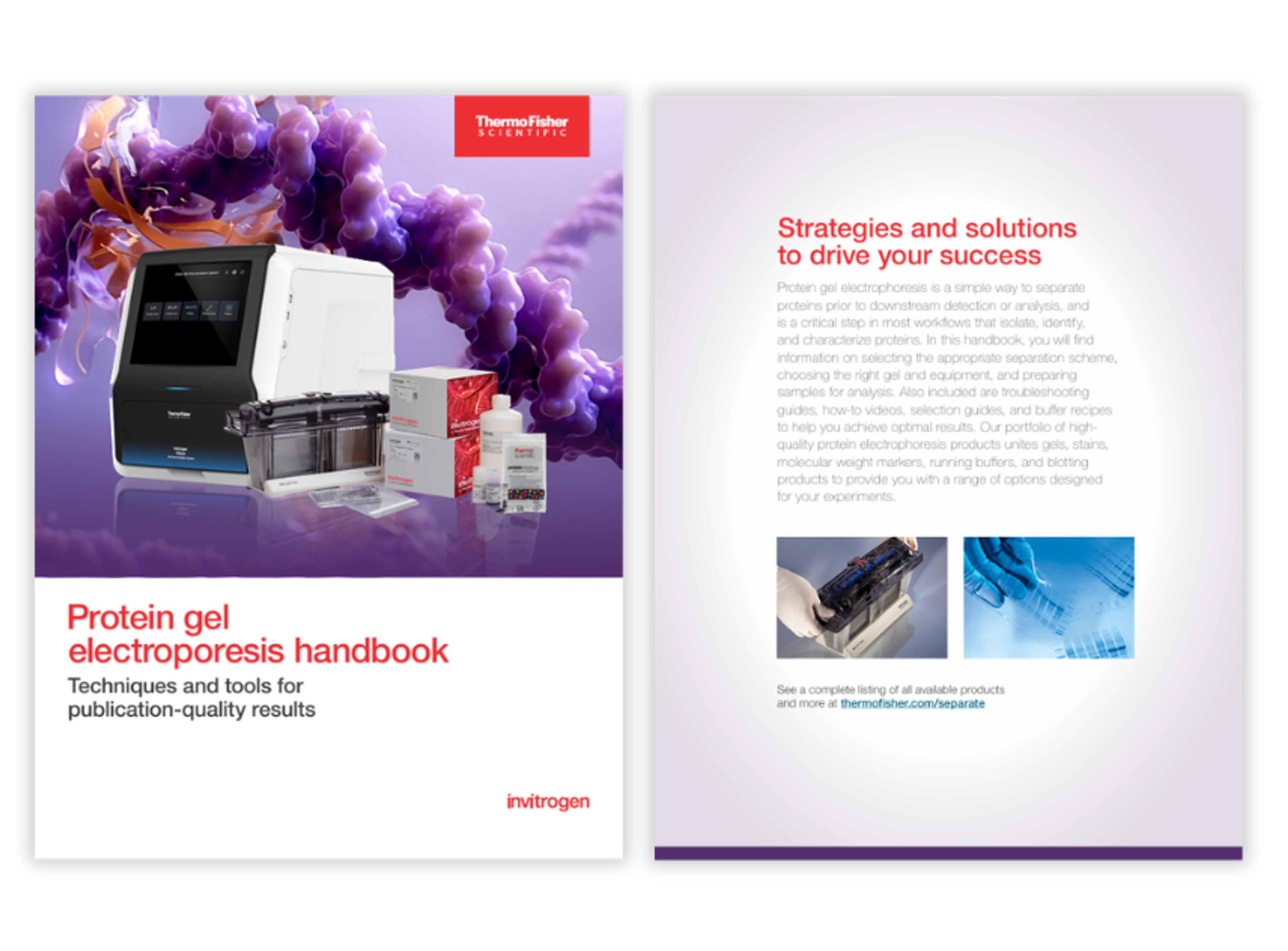
Protein gel electroporesis handbook
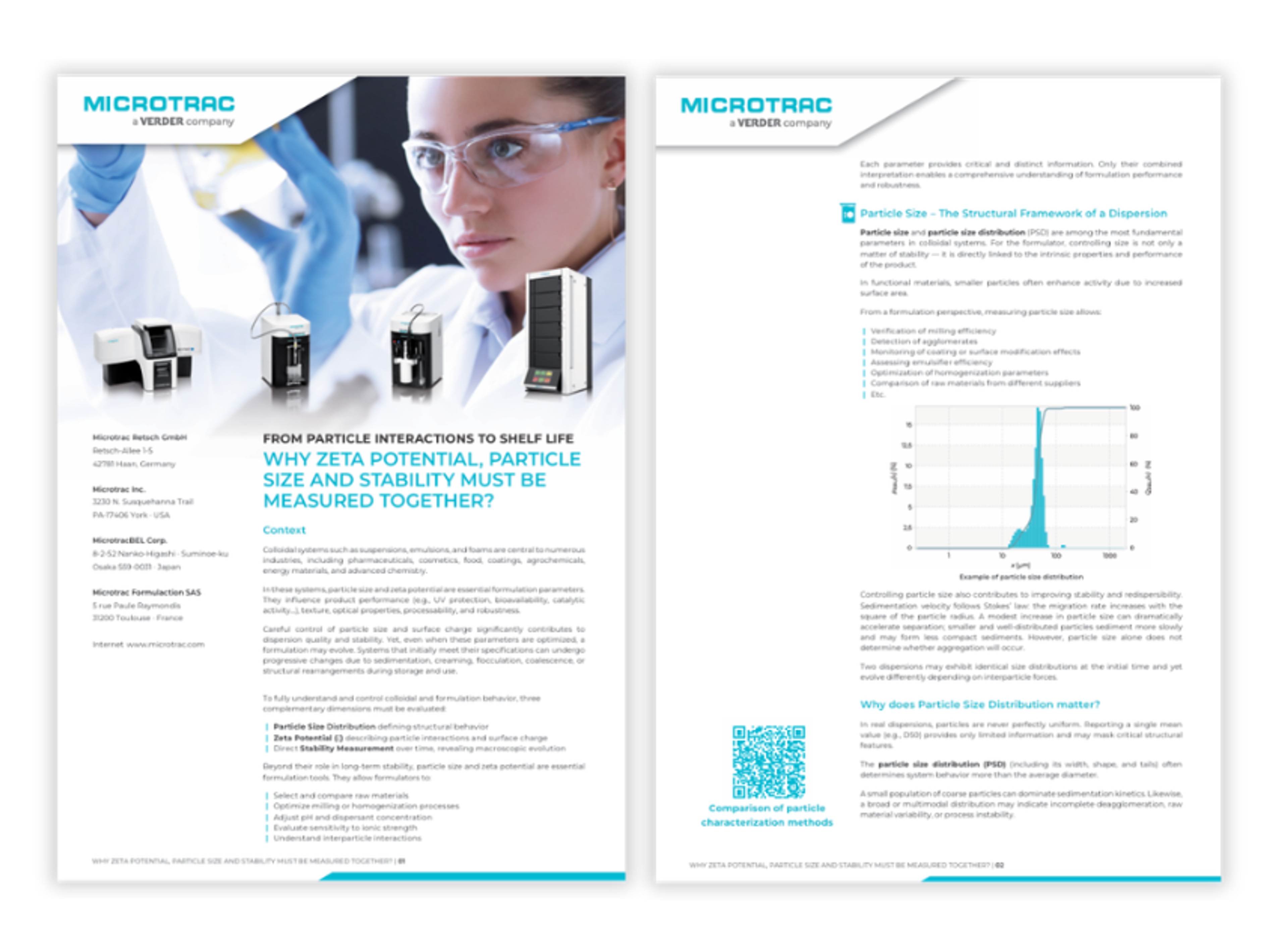
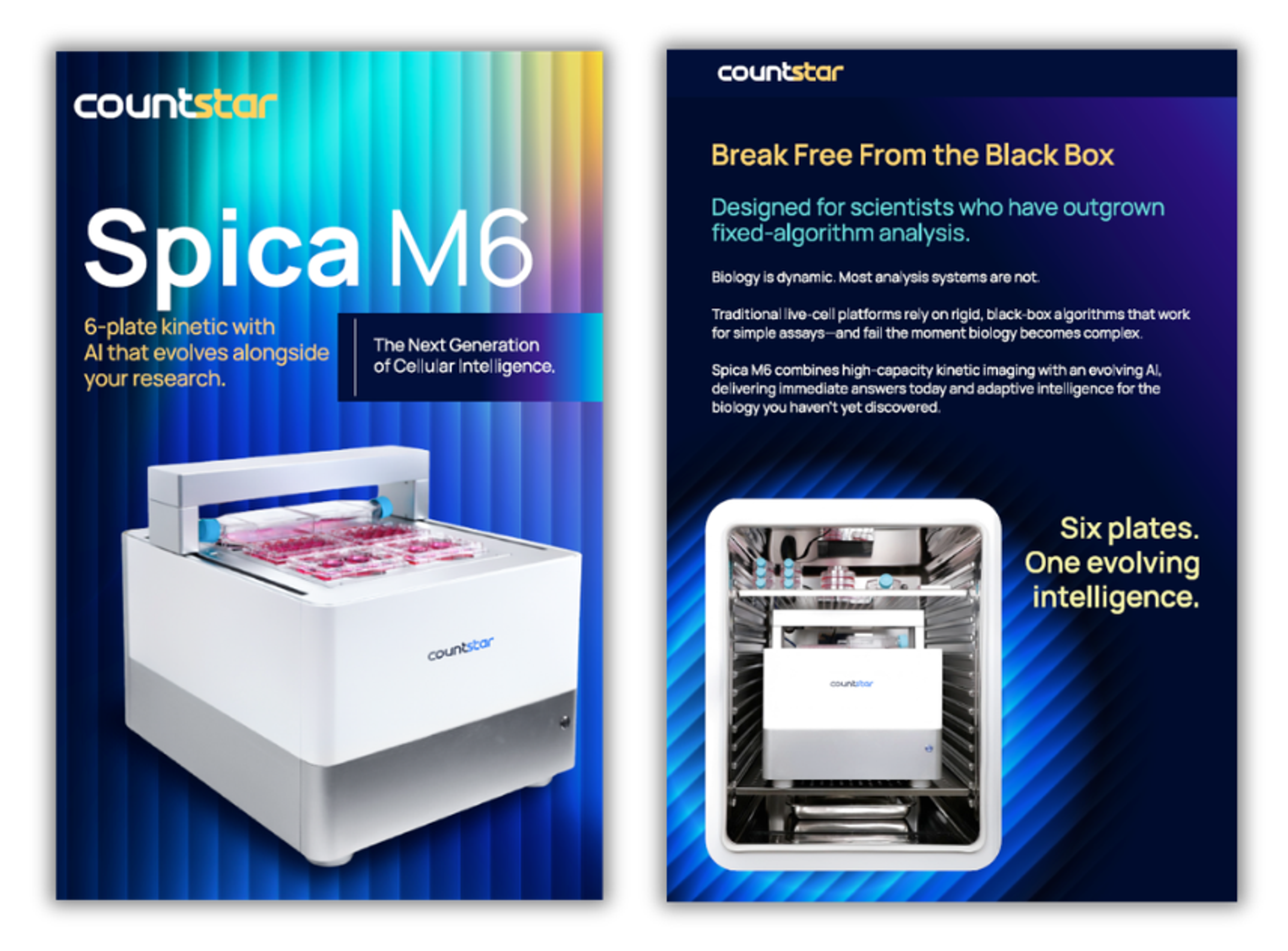
Product Brochures
Countstar Spica M6 brochure
Application Note
Spatial imaging demystified
Application Note
Cell therapy handbook
Application Note